Optical coupler

a technology of optical couplers and couplers, applied in the field of optical couplers, can solve the problems of many waveguides manufactured, reduced coupling efficiency, light loss, etc., and achieve the effect of mass production, optimized coupling efficiency, and reduced light damping in the componen

Active Publication Date: 2006-11-09
DIETRICH KLAUS +4
View PDF2 Cites 14 Cited by
  • Summary
  • Abstract
  • Description
  • Claims
  • Application Information

AI Technical Summary

Benefits of technology

[0012] It is therefore an object of the present invention to create an optical component with an optical coupling element, wherein the optical component with the optical coupling element may preferably be able to be manufactured in a simple and inexpensive manner and with a mass production, and be suitable for many different applications.
[0013] It is furthermore the object of the invention to specify a method for the manufacture of optical components, which permits an exact, mutual positioning of the waveguide and of the coupling element. The coupling efficiency is to be optimized by way of this and the light damping in the component is to be reduced to a minimum. One strives for a production which produces as little as possible rejects.
[0014] A further object of the invention is to specify methods for coupling light out of a waveguide structure or into a waveguide structure, which may also be carried out with waveguide structures which are deposited on a substrate.
[0015] These and other objects will be apparent to those skilled in this art from the following detailed description of a preferred embodiment of the invention. These and other objects are achieved by the coupling element, the optical component, the manufacturing method and the coupling-in and coupling-out method, as defined in the independent patent claims. Advantageous embodiments are specified in the dependent patent claims.
[0016] In contrast to U.S. Pat. No. 5,832,159, according to the invention, the coupling-in and coupling-out is spatially distinctly separated from the light deflection and light collimation. Observed with regard to time, the procedure of the coupling-out and coupling-in and the procedure of the light deflection and light collimation are exchanged with one another with respect to U.S. Pat. No. 5,832,150. By way of this, one succeeds in the coupling element being able to be manufactured without the waveguide structure to be coupled. The manufacture thus becomes simpler and less expensive. It may be standardized and directed to large batch numbers. The coupling element according to the invention may be used on a substrate with wave-guiding structures, for example strip waveguides (microstrips).
[0017] The optical component according to the invention contains a waveguide structure and a coupling element for the optical coupling of the waveguide structure to a further optical component. The waveguide structure and the coupling element are attached on a common substrate. The coupling element contains a reflecting, curved surface for the simultaneous change of the propagation direction and of the shape of the wave fronts of light which propagates between the waveguide structure and the optical components.

Problems solved by technology

Even a shift by a fraction of the core width leads to a considerable reduction of the coupling efficiency, and thus to light losses.
For this reason, many waveguides manufactured according to the method described in EP-0′911′658 A1 become unusable, even if one attempts to carry out the placing of the optical components and the direct writing of the waveguide structure as accurately and as reproducibly as possible.
The method thus results in a high rejection rate.
One disadvantage of this coupler is its complicated manufacture.
Furthermore, such a coupler may only be used for optical fibers which are free, but not for waveguide structures which are deposited on a substrate.
They are accordingly technically complicated and expensive in manufacture and procurement.

Method used


Image

  • Optical coupler
  • Optical coupler
  • Optical coupler

Examples


Embodiment Construction

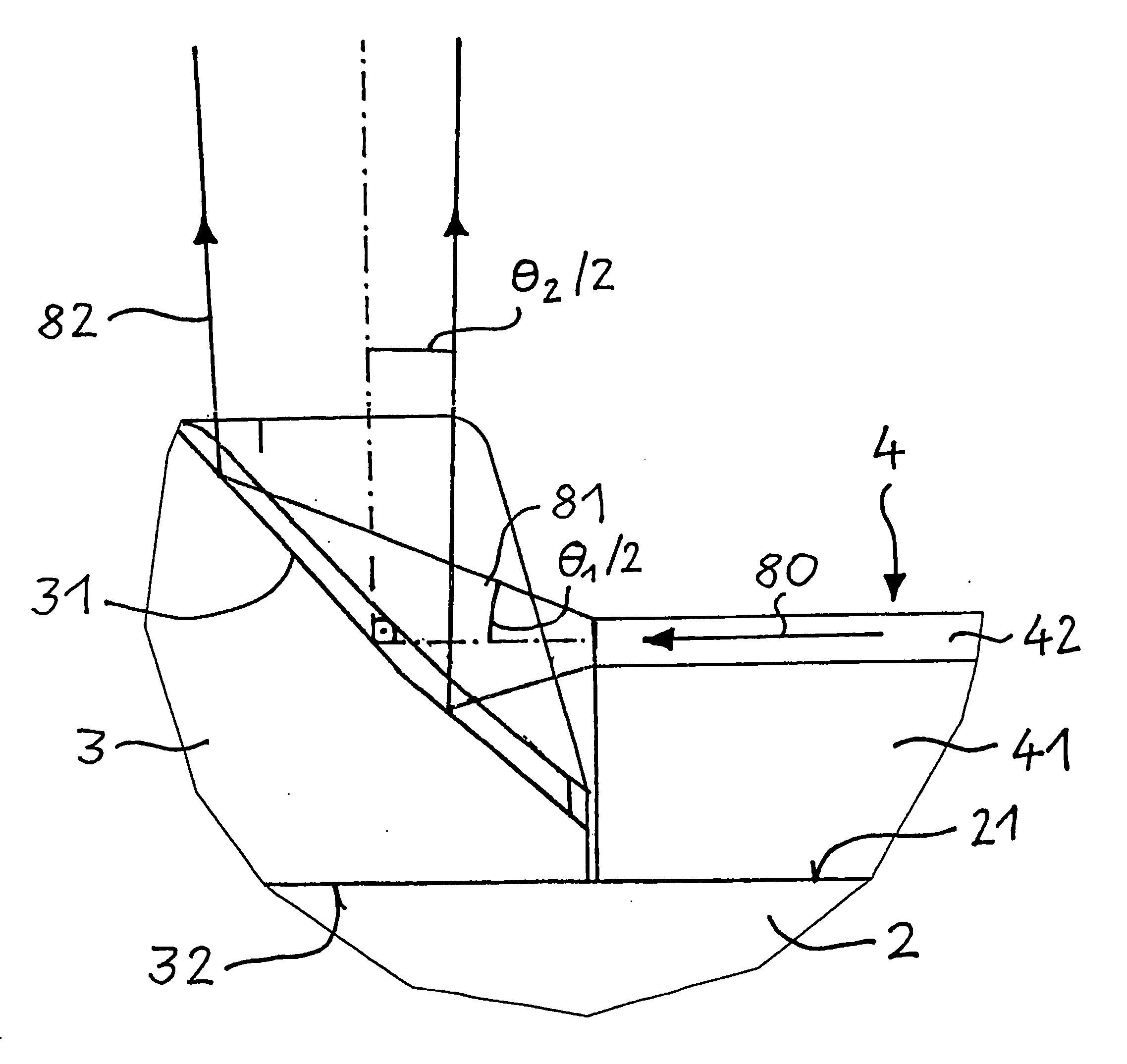
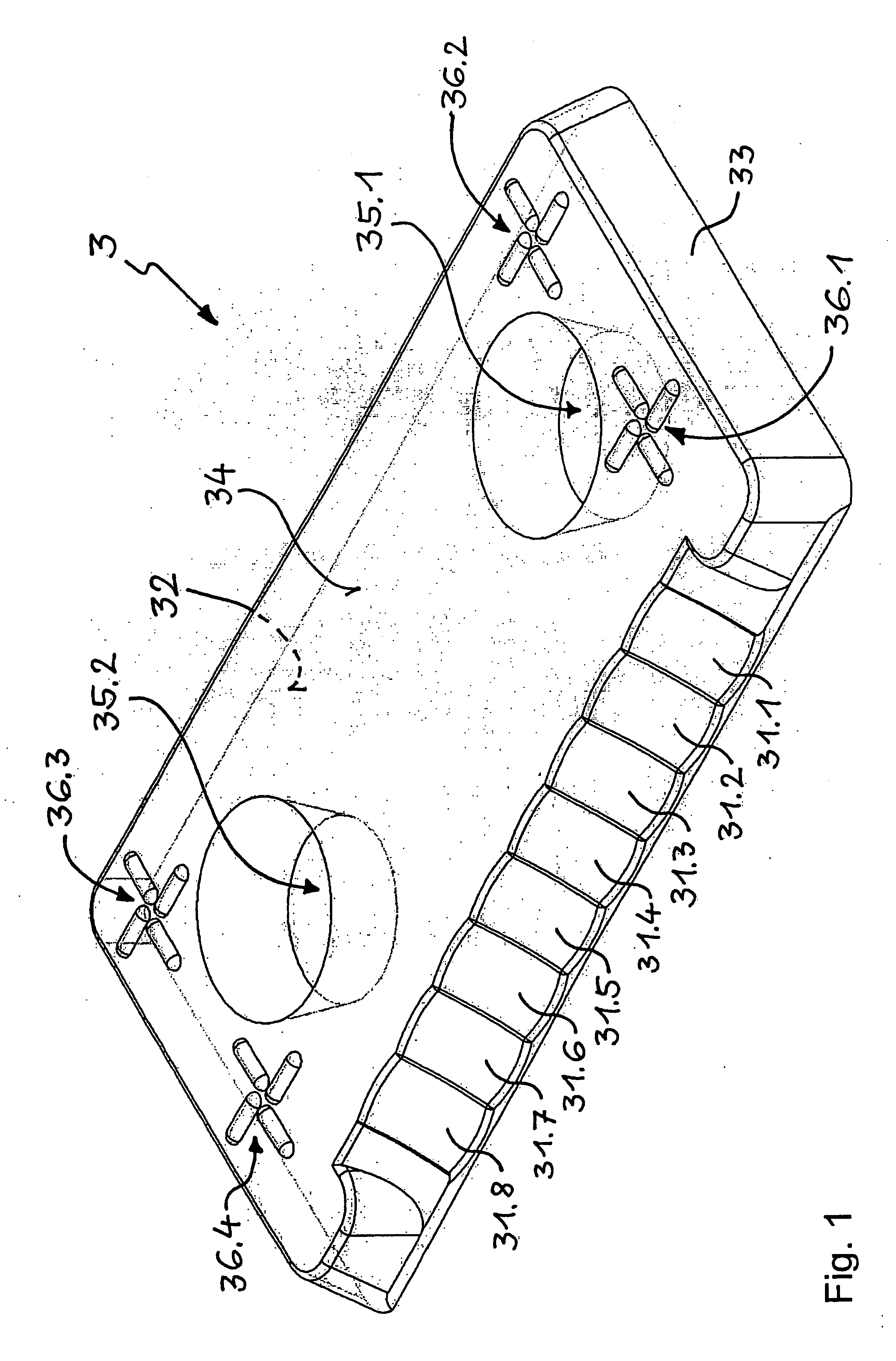
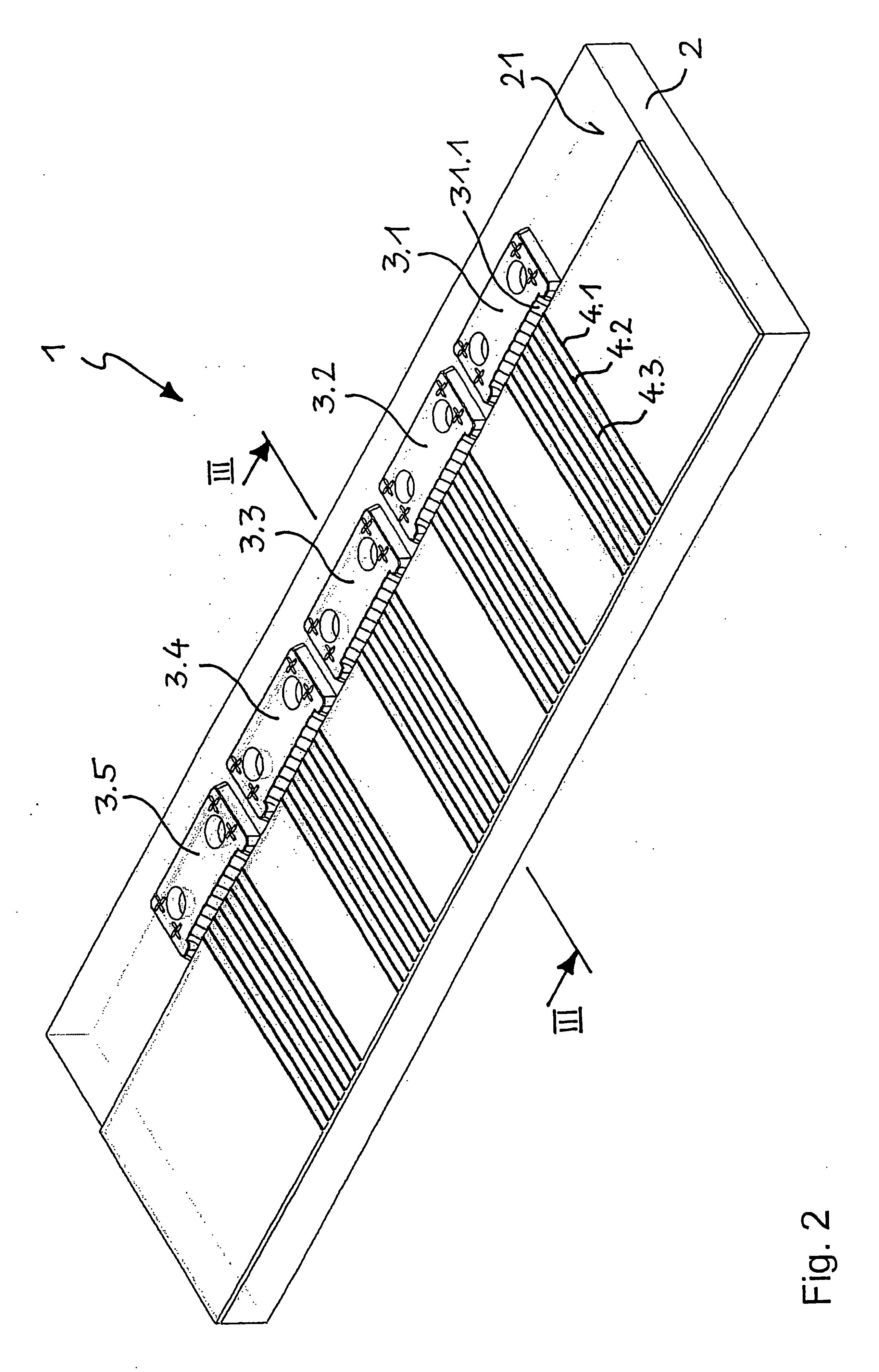
[0038]FIG. 1 shows a preferred embodiment of a coupling element 3 for the application in an optical component according to the invention. Thereby, it is the case of an autonomous element which may be manufactured inexpensively in large quantities. It may be manufactured for example by way of molding from a plastic capable of being injection molded, such as polycarbonate (PC), polymethylmethacrylate (PMMA) or polyetheretherketone (PEEK). Standardized components may be produced with this method in large batch numbers and with strict tolerances and at low costs. One may apply methods such as micro-embossing or micro-injection-molding, in order to manufacture structures with dimension of a few 100 μm.

[0039] The basic shape of the coupling element 3 may for example be a truncated pyramid with a rectangular base surface 32, wherein the base surface 32 may measure approx. 6 mm×3 mm and the height may amount to approx. 0.5 mm. In the embodiment example of FIG. 1, the coupling element 3 is ...


PUM


Abstract

A coupling element (3) and a waveguide structure (4) are deposited on a common substrate (2) of an optical component (1). The coupling element (3) serves for the optical coupling of the waveguide structures (4) to a further optical component. The coupling element (3) contains a reflecting, curved surface (31.1-31.8) for deflecting and for collimation of light which propagates between the waveguide structure 4 and the further optical component. The coupling element (3) creates a standard for interfaces between the optical component (1) and a further optical component. The manufacture of the coupling element (3) is simple and inexpensive, may be standardized and directed to large batch numbers.

Description

CROSS-REFERENCE TO RELATED APPLICATION [0001] This application claims priority from Swiss patent application No. CH 00690 / 05, filed Apr. 18, 2005. BACKGROUND OF THE INVENTION [0002] 1. Technical Field [0003] The invention lies in the field of optical couplers for optical waveguides and relates to an optical component, a method for manufacturing an optical component and a method for coupling light out of a waveguide structure or into a waveguide structure, according to the preambles of the independent patent claims. The optical components according to the invention may have extensions in the region of a few centimeters to a few meters. Such optical components are mainly required for optical data transmission, and are applied for example in telecommunication, medical technology, sensor technology, in the construction of vehicles and aircraft, in technology relating to industry, buildings and control. Particularly advantageous embodiments are circuit boards which comprise electrical as...

Claims


Application Information

Patent Timeline
Patent Type & Authority Applications(United States)
IPC IPC(8): G02B6/26
CPCG02B6/138G02B6/4221G02B6/4214
Inventor DIETRICH, KLAUSHALTER, MARKUSMICHLER, MARKUSPAREDES, STEPHANWALSER, ANDREAS
Owner DIETRICH KLAUS
Why Eureka
Try Eureka