Imaging apparatus

a technology of imaging apparatus and fixing member, which is applied in the direction of radiation control devices, instruments, exposure control, etc., can solve the problems of preventing high image quality, degrading image quality, and reducing image quality, so as to reduce the anisotropy of the fixing member or substrate, and eliminate the thermal expansion anisotropy of the adhesiv

Active Publication Date: 2006-11-09
PANASONIC CORP
View PDF9 Cites 23 Cited by
  • Summary
  • Abstract
  • Description
  • Claims
  • Application Information

AI Technical Summary

Benefits of technology

[0016] This configuration can eliminate thermal expansion anisotropy of the adhesive to reduce anisotropy of the fixing member or substrate to be glued. In this way, the fixing member or substrate can be strengthened and the imaging apparatus can be thinned down.

Problems solved by technology

This optical filter is fixed by an adhesive, dust generated from which may also cause degradation in image quality of the imaging apparatus and may prevent high image quality even if dirt generated in the assembly environment is reduced.
Specifically, filler contained in the adhesive may be released at the time of adhesion of the optical filter or may drop after cure of the adhesive, so that a problem occurs that the released or dropped filler sticks to the incident surface of the semiconductor imaging device and degrades image quality.

Method used


Image

  • Imaging apparatus
  • Imaging apparatus
  • Imaging apparatus

Examples


Embodiment Construction

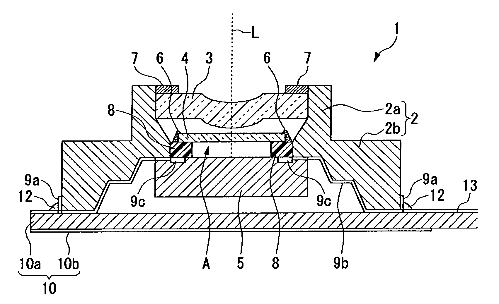
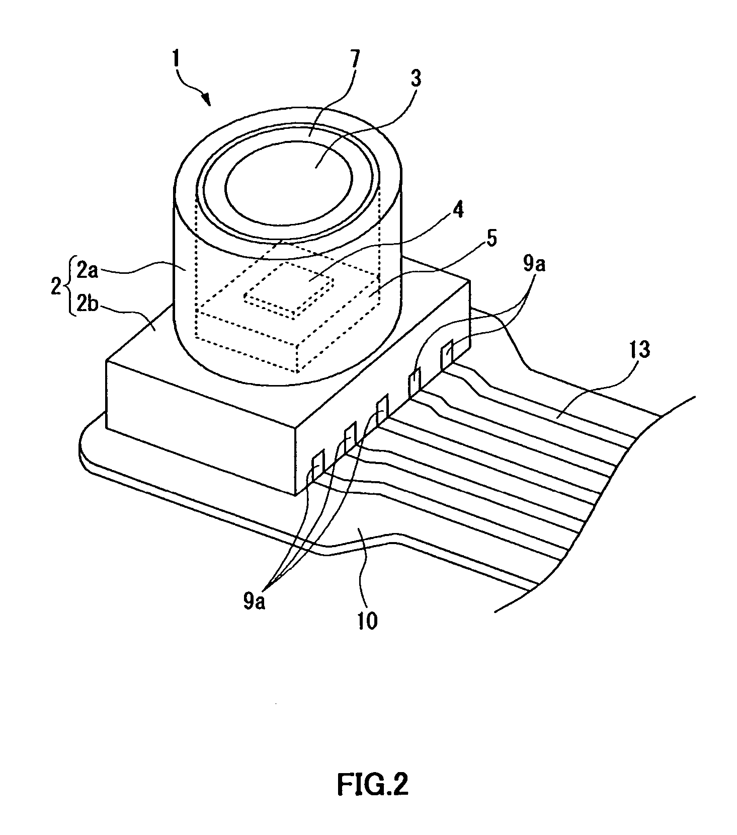
[0023] An imaging apparatus according to an embodiment of the invention will now be described referring to the drawings. If possible, the same parts are designated by the same letters and are not described repeatedly.

[0024]FIG. 1 shows a cross section of an imaging apparatus 1 according to an embodiment, FIG. 2 shows a perspective view of the imaging apparatus 1, and FIG. 3 is an exploded perspective view of the major part of the imaging apparatus 1 shown in FIG. 2 when seen from the back. As shown in FIG. 1, the imaging apparatus 1 according to the embodiment has an aspherical lens 3, an optical filter 4, a semiconductor imaging device 5, which are placed along an optical axis L; a three-dimensional substrate 2 fixing these three, and a printed circuit board (FPC) 10 connected to the three-dimensional substrate 2. In this embodiment, the three-dimensional substrate 2 has a role in fixing the semiconductor imaging device 5 along with a role as a fixing member to fix the optical fil...


PUM


Abstract

The imaging apparatus 1 comprises: a semiconductor imaging device 5 which converts incident light to an electrical signal; an optical filter 4 which is opposed to an incident surface of the semiconductor imaging device 5 and transmits light of a certain wavelength; and a three-dimensional substrate 2 fixing the optical filter 4 by means of adhesion using a filler-containing adhesive 6; wherein the diameter of the filler is smaller than or equal to the pixel size of the semiconductor imaging device 5. Degradation of image quality of the imaging apparatus 1 caused by the dropped filler can thus be reduced.

Description

TECHNICAL FIELD [0001] The present invention relates to an imaging apparatus using a semiconductor imaging device, the imaging apparatus used as a camera for a portable device or the like. BACKGROUND ART [0002] As described in Japanese Patent Laid-Open Application No. 2001-245186 etc., previously known is an imaging apparatus configured to convert an image, imaged by a lens, to an electrical signal using a CCD or other semiconductor imaging device so as to capture the image. With demand for smaller and more sophisticated portable devices, imaging apparatuses have been required to be even smaller and lighter in weight. Accordingly, imaging apparatuses have been made thinner by thinning each component. On the other hand, the number of pixels has been increased in accordance with requirements for high image quality, and therefore the size of a pixel has also been miniaturized. [0003] In the field of imaging apparatuses, a black or white dot or the like on an image caused by a flaw in a...

Claims


Application Information

Patent Timeline
Patent Type & Authority Applications(United States)
IPC IPC(8): G03B7/099H01L27/146H01L27/14H01L31/0203H01L31/0232H04N5/225H04N5/335
CPCH01L27/14618H01L27/14625H04N5/2254H01L31/0232H04N5/2253H01L31/0203H01L2924/0002H01L31/02325H04N23/54H04N23/57H04N23/55H01L2924/00H01L27/14H04N23/00
Inventor NISHIZAWA, HIROSHI
Owner PANASONIC CORP
Why Eureka
Try Eureka