Film pattern, device, electro-optic device, electronic apparatus, method of forming the film pattern, and method of manufacturing active matrix substrate

Inactive Publication Date: 2006-11-16
SEIKO EPSON CORP
View PDF10 Cites 12 Cited by
  • Summary
  • Abstract
  • Description
  • Claims
  • Application Information

AI Technical Summary

Benefits of technology

[0011] In consideration of the circumstance described above, the invention has an advantage of providing a method of forming a film pattern capable of eliminating a surface process (lyophobic process) to the bank, there

Problems solved by technology

However, if it is attempted to form such fine wiring patterns by the manufacturing method using the droplet discharge process, it is particularly difficult to obtain a sufficient preciseness in the width of the wiring.
Further, if it is attempted that the wiring pattern is formed using the droplet discharge process, a thermal process with relatively high temperature is required especially from necessity of burning conductive micro particles as a functional material for forming the wiring pattern.
However, especially in the case in which the wiring pattern is formed using the bank, the bank made of an organic material typically used, which has poor resistance to the thermal process, sometimes causes a problem of meltdown during the thermal process.
However, the bank

Method used


Image

  • Film pattern, device, electro-optic device, electronic apparatus, method of forming the film pattern, and method of manufacturing active matrix substrate
  • Film pattern, device, electro-optic device, electronic apparatus, method of forming the film pattern, and method of manufacturing active matrix substrate
  • Film pattern, device, electro-optic device, electronic apparatus, method of forming the film pattern, and method of manufacturing active matrix substrate

Examples


Example

First Embodiment

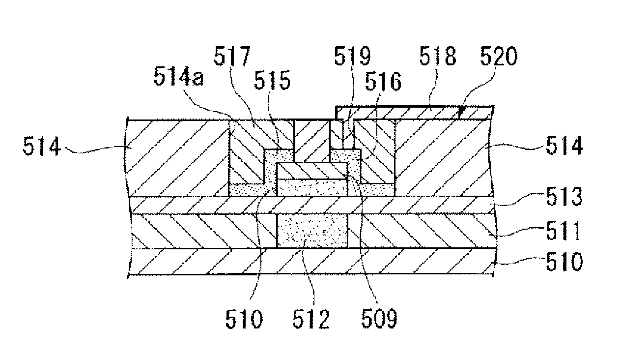
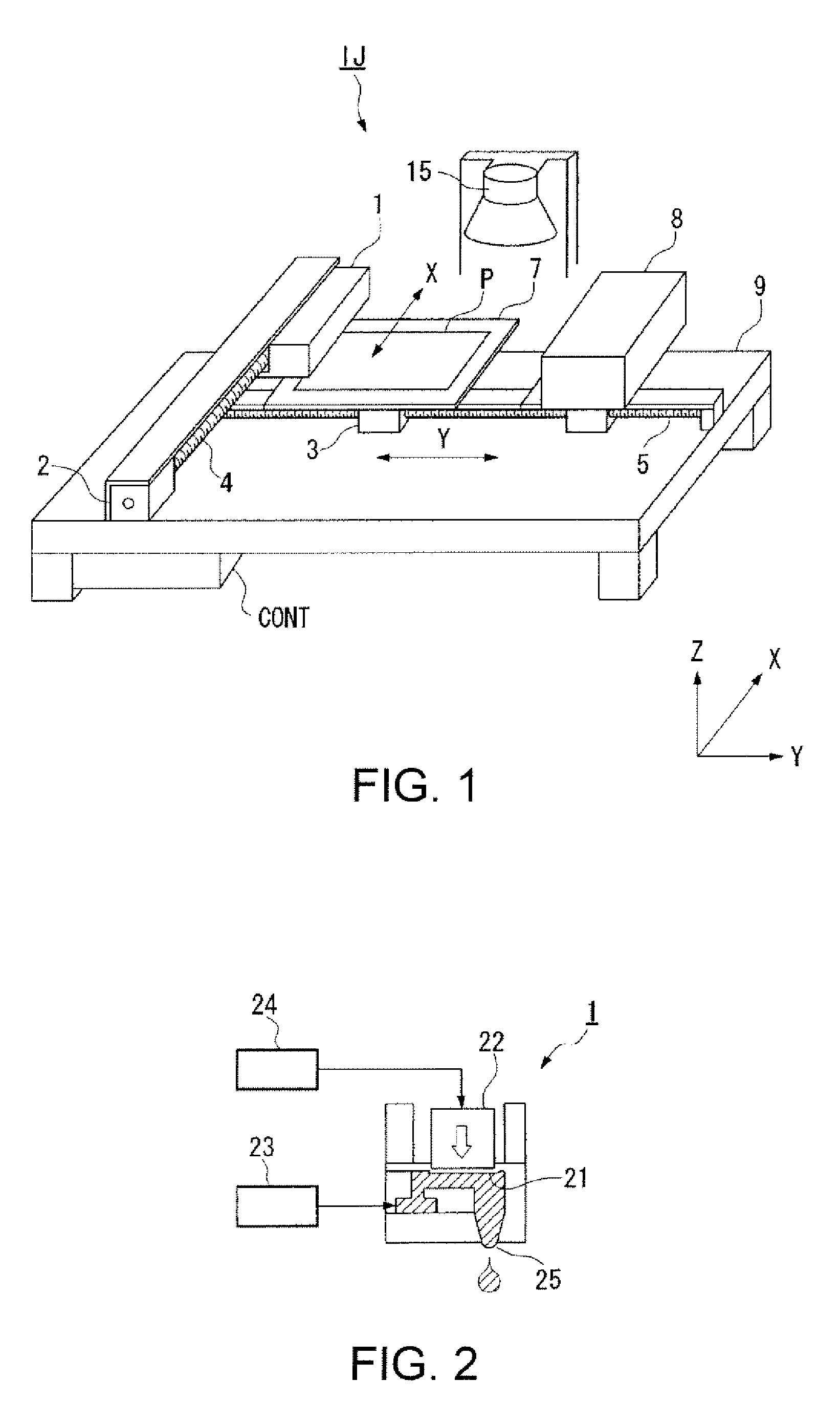
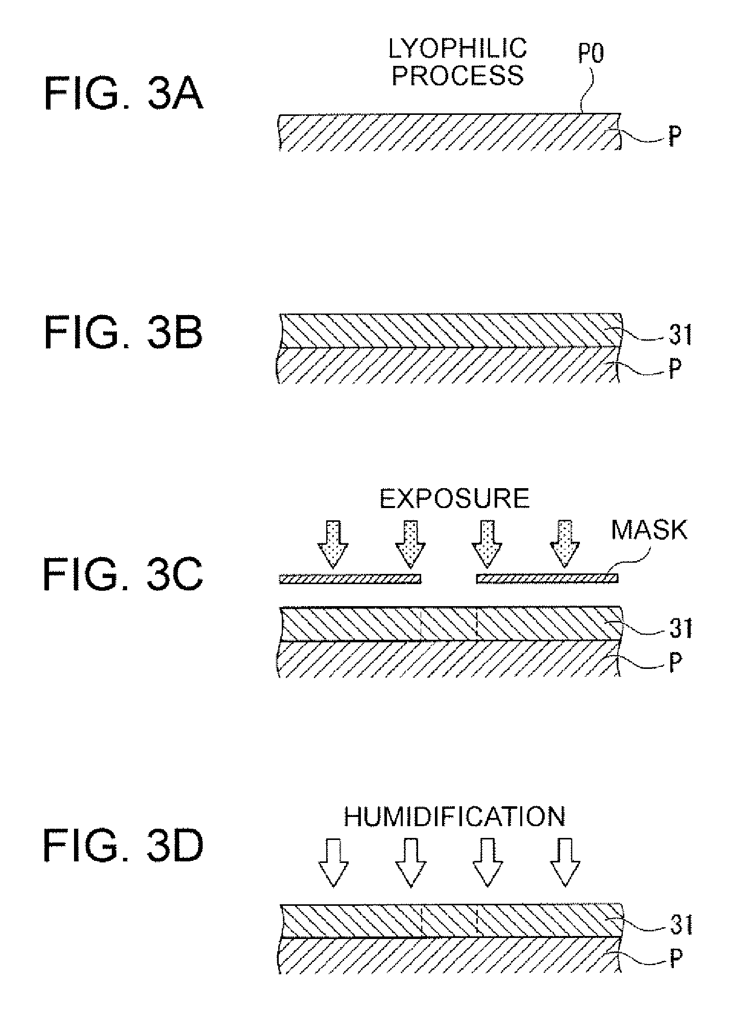
[0074] Firstly, a method of forming a film pattern according to a first embodiment of the invention will be explained, in which ink (functional liquid) for forming a wiring pattern (the film pattern) containing conductive micro particles is discharged as a droplet from a discharging nozzle of a droplet discharging head to form the wiring pattern (the film pattern) between the banks, namely in an area partitioned by the banks which are formed on the substrate in accordance with the wiring pattern. It is assumed in the embodiment that the wiring pattern (the film pattern) composed of a plurality of layers stacked one another is formed by especially discharging two kinds of functional liquid different from each other.

[0075] As the ink (the functional liquid) for forming the wiring pattern, in consideration that the bank made of a material having the siloxane bond with hydrophobicity such as poly-methyl siloxane as the framework, namely the bank made of poly-siloxane a...

Example

Second Embodiment

[0145] As a second embodiment, the wiring pattern 33 having a different configuration from the first embodiment will be explained with reference to FIG. 7. Note that in the second embodiment, different sections from the first embodiment will be explained.

[0146] In the present second embodiment, wiring pattern ink X3 using titanium as the conductive micro particles and the wiring pattern ink X2 using silver as the conductive micro particles are stacked in the film pattern forming area 34 by repeatedly performing the material disposing step and the preliminary drying step explained in the first embodiment as shown in FIG. 7. Note that as shown in the drawings, the wiring pattern ink X3, the wiring pattern ink X2, and again the wiring pattern ink X3 are stacked in the film pattern forming area 34 in this order from the side of the substrate P. Namely, the wiring pattern ink X2 is disposed in the film pattern forming area 34 so as to be sandwiched by the layers of the...

Example

Third Embodiment

[0150] As a third embodiment, the wiring pattern 33 having a different configuration from the first embodiment and the second embodiment will be explained with reference to FIG. 8. Note that in the third embodiment, different sections from the first embodiment will be explained.

[0151] In the present third embodiment, the wiring pattern ink X1 using chromium as the conductive micro particles and the wiring pattern ink X2 using silver as the conductive micro particles are stacked in the film pattern forming area 34 by repeatedly performing the material disposing step and the preliminary drying step explained in the first embodiment as shown in FIG. 8. Note that as shown in the drawings, the wiring pattern ink X1, the wiring pattern ink X2, and again the wiring pattern ink X1 are stacked in the film pattern forming area 34 in this order from the side of the substrate P. Namely, the wiring pattern ink X2 is disposed in the film pattern forming area 34 so as to be sandw...


PUM


Abstract

A method of forming a film pattern by disposing a functional liquid on a substrate includes a step of forming a bank on the substrate, the bank corresponding to an area on which the film pattern is to be formed, a step of disposing the functional liquid to the area partitioned by the bank, and a step of curing the functional liquid to form the film pattern, one of a polysilazane liquid and a polysiloxane liquid is applied, exposed, developed, patterned, and burnt, thereby forming the bank made of a material having a hydrophobic group in the side chain and a siloxane bond as a framework in the step of forming the bank, and a liquid containing one of a water type dispersion medium and a water type solvent is used as the functional liquid.

Description

BACKGROUND OF THE INVENTION [0001] 1. Technical Field [0002] The present invention relates to a film pattern, a device, an electro-optic device, an electronic apparatus, a method of forming the film pattern, and a method of manufacturing an active matrix substrate. [0003] 2. Related Art [0004] In the past, a photolithography process has been frequently used for manufacturing fine wiring patterns (film patterns) used in, for example, a semiconductor integrated circuit. In contrast, in recent years, a manufacturing method using a droplet discharge process has been proposed. In this manufacturing method, a functional liquid (ink for forming a wiring pattern) containing a functional material (conductive micro particles) for forming the wiring pattern is discharged from a droplet discharging head on to a substrate to dispose the material on a pattern forming surface, thereby forming the wiring pattern. And the manufacturing method is considered to be very effective because it can cope wi...

Claims


Application Information

Patent Timeline
IPC IPC(8): G02F1/136
CPCG02F1/1368G02F1/136H01L27/1214H05K3/1258H05K2203/013H10K71/135H10K59/122
Inventor HIRAI, TOSHIMITSUMORIYA, KATSUYUKI
Owner SEIKO EPSON CORP
Why Eureka
Try Eureka