Optical device with slab waveguide and channel waveguides on substrate

a technology of optical devices and substrates, applied in the field of optical signal processing, can solve the problems of large thickness of the entire device, difficult to achieve high resolution and miniaturization, and difficult to thin the diffraction grating, and achieve the effect of flattop transmission properties and small loss

Inactive Publication Date: 2006-11-16
FUJITSU LTD
View PDF4 Cites 24 Cited by
  • Summary
  • Abstract
  • Description
  • Claims
  • Application Information

AI Technical Summary

Benefits of technology

[0077] The present invention was conceived with consideration of such problems, and its purpose is to provide a compact optical functional device that has flattop type transmission properties and has little loss.

Problems solved by technology

With the first conventional example shown in FIG. 2, it is difficult to achieve high resolution and miniaturization, which are required in WDM systems.
In contrast to this, as stated previously, it is difficult to make thin the diffraction gratings and lenses used in spatial join type wavelength selective switches, so there is the problem in which the thickness of the entire device becomes large.
Therefore, there is the problem that assembly is troublesome in comparison to the waveguide type wavelength selective switch.
This high insertion loss is a problem.
In the example of FIG. 3, for example, it passes through the AWGs twice, so this results in a loss increase of approximately 6 dB.

Method used


Image

  • Optical device with slab waveguide and channel waveguides on substrate
  • Optical device with slab waveguide and channel waveguides on substrate
  • Optical device with slab waveguide and channel waveguides on substrate

Examples


example of embodiment 1

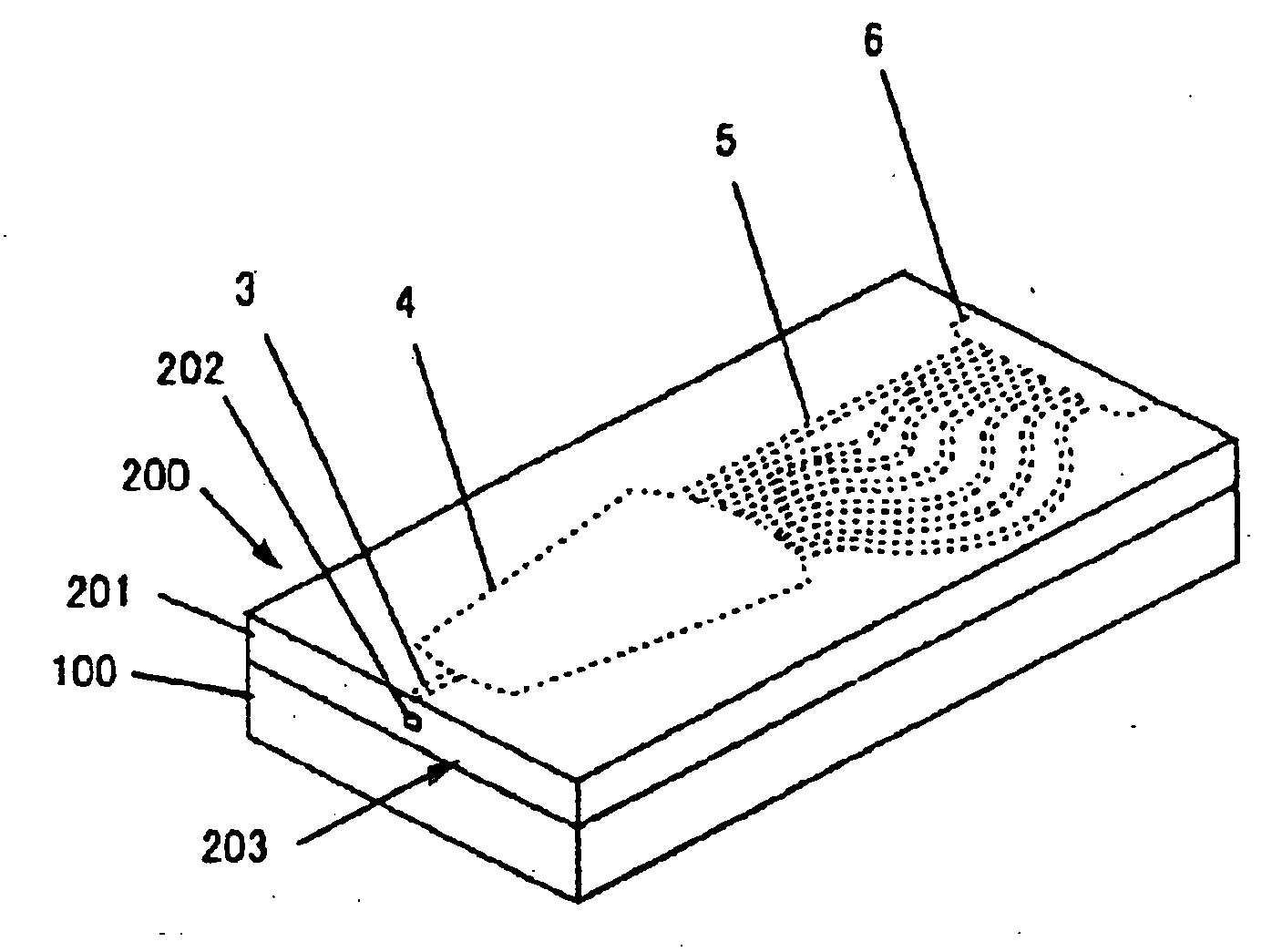
[0173]FIG. 13 is an example of the optical functional device of the present invention, and it is an example of a wavelength combining / branching filter configuration. FIG. 13(a) is a plan view of the wavelength combining / branching filter, FIG. 13(b) is a cross-sectional view in which the wavelength combining / branching filter is cut by dotted line A-A of FIG. 13(a), FIG. 13(c) is a cross-sectional view in which the wavelength combining / branching filter is cut by dotted line B-B of FIG. 13(a), and FIG. 13(d) is a cross-sectional view in which the wavelength combining / branching filter is cut by dotted line C-C of FIG. 13(a).

[0174] As shown in FIG. 13(b), for example, the wavelength combining / branching filter of the present invention is comprised of slab substrate 100 and light guide 200 that is formed on the primary plane of slab substrate 100. Here, the “primary plane” of slab substrate 100 is the surface that makes contact with light guide 200 in slab substrate 100 of FIG. 13(b), for...

example of embodiment 2

[0202]FIG. 15 and FIG. 16 show an example of embodiment of the optical functional device of the present invention. FIG. 15 shows a plan view of a wavelength selective switch that is applied to 40-channel wavelength division multiplexed light with frequency intervals of 100 GHz, and FIG. 16 shows the side view thereof.

[0203]FIG. 17 is an enlarged drawing of part A of FIG. 15, and it schematically shows the exit directions of light with each wavelength when light that is wavelength-multiplexed with 100 GHz frequency intervals (equivalent to wavelength intervals of approximately 0.8 nm in the 1.5 μm wavelength region) is emitted from channel waveguide array 5.

[0204] In FIG. 15 and FIG. 16, the first combining / branching device 20 and the second combining / branching device 21 for 100 GHz frequency intervals are mounted on thermal conduction fin 10, which is mounted on heater 22.

[0205] These combining / branching devices 20 and 21 have identical structures, and they are comprised of input...

example of embodiment 3

[0231]FIG. 19 and FIG. 20 show an example of embodiment of the optical functional device of the present invention. FIG. 19 shows a plan view of a wavelength selective switch that is applied to 40-channel wavelength division multiplexed light with frequency intervals of 100 GHz, and FIG. 20 shows the side view thereof.

[0232]FIG. 21 is an enlarged drawing of part A of FIG. 19, and it schematically shows the exit directions of light with each wavelength when light that is wavelength-multiplexed with 100 GHz frequency intervals (equivalent to wavelength intervals of approximately 0.8 nm in the 1.5 μm wavelength region) is emitted from output slab waveguide 6.

[0233] This example of embodiment is a configuration that is similar to Example of Embodiment 2, but it differs in that (a) the combining / branching device is directly mounted on heater 22, without establishing a thermal conduction fin on which to mount the combining / branching device, and (b) a short output slab waveguide 6 having ...


PUM


Abstract

An optical device used, for example, in an add / drop multiplexer, a dynamic gain equalizer or a optical power monitor. The optical device includes (a) a substrate; (b) a first slab waveguide formed on the substrate; (c) channel waveguides of differing lengths formed on the substrate, light output from the first slab waveguide being input to the channel waveguides; and (d) a second slab waveguide formed on the substrate, light output from the channel waveguides being input to the second slab waveguide. An end face of the second slab waveguide shares a face with an end face of the substrate. The optical device has low loss characteristics.

Description

CROSS-REFERENCE TO RELATED APPLICATIONS [0001] The present application claims priority to Japanese application 2003-026614, filed Feb. 4, 2003, and which is incorporated herein by reference, in its entirety. BACKGROUND OF THE INVENTION [0002] 1. Field of the Invention [0003] The present invention relates to optical signal processing for the purpose of performing signal pathway switching and light output power adjustment for each wavelength in a WDM (Wavelength Division Multiplexing) system. More particularly, it is related to an optical functional device that uses flat light guides to integrate and miniaturize components that are necessary for the adding and dropping of signals with specific wavelengths, the adjustment and monitoring of light output power for each wavelength, and wavelength dispersion compensation for each wavelength. [0004] 2. Description of the Related Art [0005] In recent years, the introduction of WDM systems has been aggressively advanced in order to accommodat...

Claims


Application Information

Patent Timeline
Patent Type & Authority Applications(United States)
IPC IPC(8): G02B6/12G02B6/28G02B6/34G02B26/08
CPCG02B6/12011G02B6/29383G02B6/12019G02B6/28
Inventor TABUCHI, HARUHIKONARUSE, TERUKAZUTERADA, KOJISHIBATA, KOHEI
Owner FUJITSU LTD
Why Eureka
Try Eureka