

Bank structure, wiring pattern forming method, device, electro-optical device, and electronic apparatus
a pattern forming and wire pattern technology, applied in the field of wire pattern forming method, device, electrooptical device, electronic apparatus, can solve the problems of short circuit, high manufacturing cost, wire breakage, etc., and achieve the effect of increasing electrical resistance, large cross-sectional shape, and wide width
- Summary
- Abstract
- Description
- Claims
- Application Information
AI Technical Summary
Benefits of technology
Problems solved by technology
Method used
Image

Examples
first embodiment
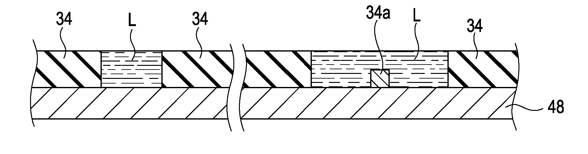
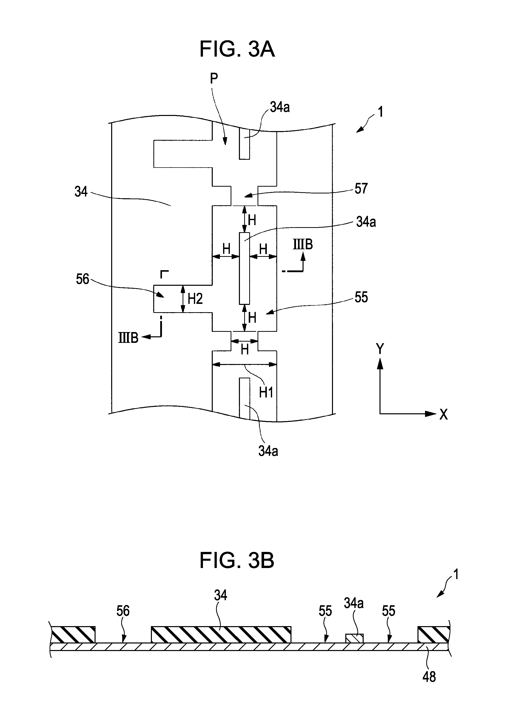
[0050] Hereinafter, one embodiment of the invention will be described with reference to the accompanying drawings. In addition, the embodiment to be described below shows some aspects of the invention, but the invention is not limited to the aspects. In addition, scales of individual layers and members in all the drawings to be used for the description below are appropriately changed so that the individual layers and members have recognizable sizes in the drawings.
Droplet Discharge Apparatus
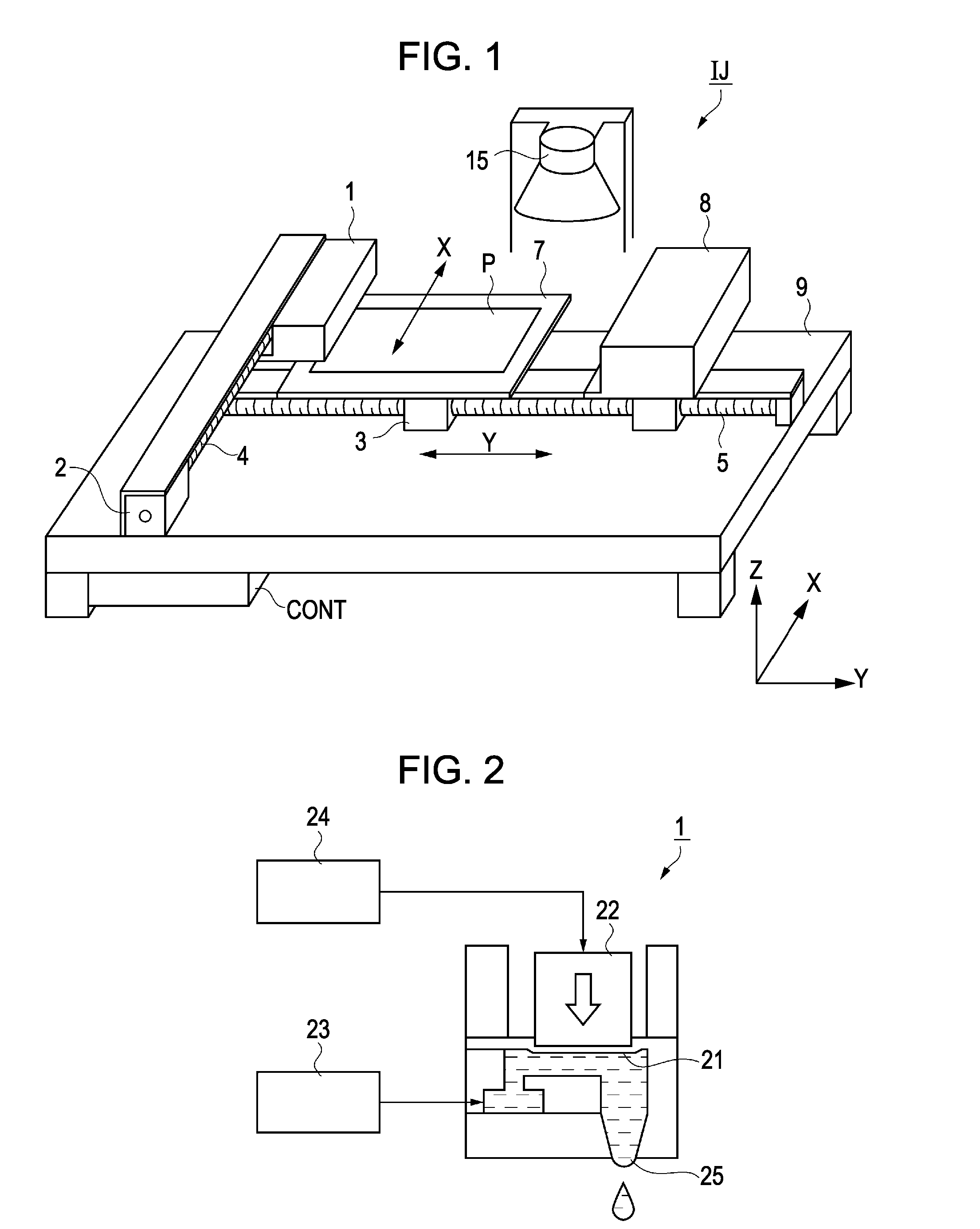
[0051] First, in this embodiment, a droplet discharge apparatus for forming a film pattern will be described with reference to FIG. 1.
[0052]FIG. 1 is a perspective view showing a schematic configuration of a droplet discharge apparatus (ink jet apparatus) IJ which arranges a liquid material onto a substrate by a droplet discharge method as an example of an apparatus used for a film pattern forming method of the invention.
[0053] The droplet discharge apparatus IJ includes a droplet discharge ...
PUM
| Property | Measurement | Unit |
|---|---|---|
| diameter | aaaaa | aaaaa |
| diameter | aaaaa | aaaaa |
| surface tension | aaaaa | aaaaa |
Abstract
Description
Claims
Application Information