Apparatus and method for processing a substrate

a substrate and apparatus technology, applied in the direction of transportation and packaging, nuclear engineering, railway signalling, etc., can solve the problems inability to prevent ambient temperature rise due to components within the chamber, and largely change the electrical properties of semiconductor devices. , to achieve the effect of small thickness difference, small difference in film thickness between the first substrate and thereafter

Inactive Publication Date: 2008-02-14
PANASONIC CORP
View PDF3 Cites 7 Cited by
  • Summary
  • Abstract
  • Description
  • Claims
  • Application Information

AI Technical Summary

Benefits of technology

[0016]The difference in the film thickness between the first substrate and thereafter can be reduced using the technique to preheat the interior of the chamber before the oxidization process starts. However, even if this technique is used, for example, when a relatively large number of, for example 25, substrates 13 are processed in succession, the oxide films of the first processed substrate and the 25th processed substrate have slightly different thicknesses (for example, approximately 0.2 nm). This is a very small difference in thickness. However, in case of forming ultrathin gate oxide films, the small difference in thickness largely changes the electrical properties of the semiconductor devices.

Problems solved by technology

However, in case of forming ultrathin gate oxide films, the small difference in thickness largely changes the electrical properties of the semiconductor devices.
Then, the rise in the ambient temperature due to the components within the chamber cannot be prevented.

Method used


Image

  • Apparatus and method for processing a substrate
  • Apparatus and method for processing a substrate
  • Apparatus and method for processing a substrate

Examples


Embodiment Construction

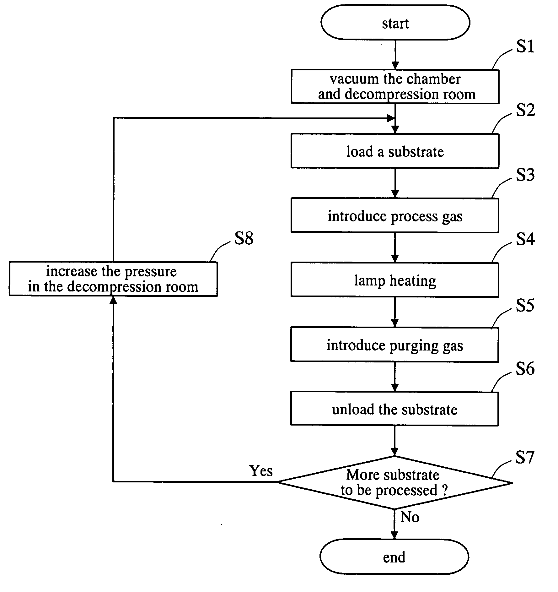
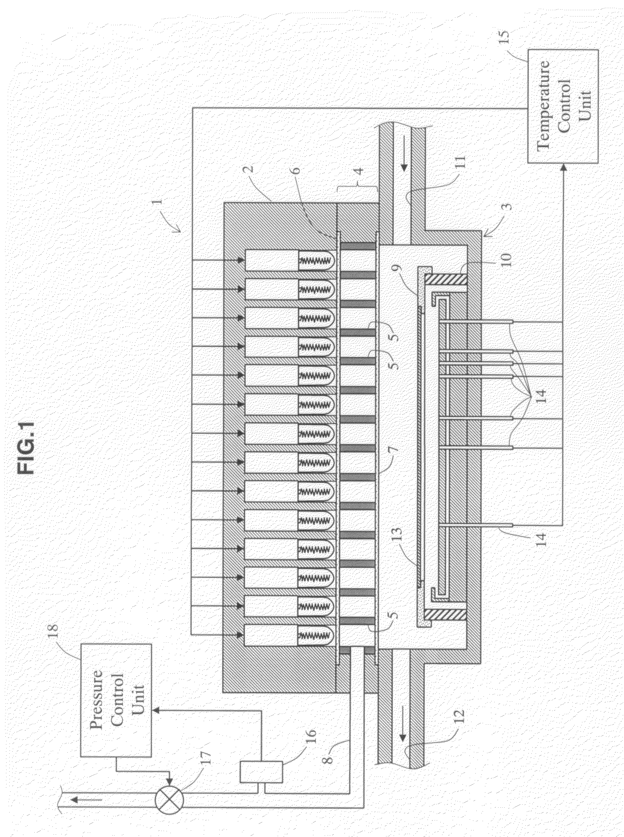
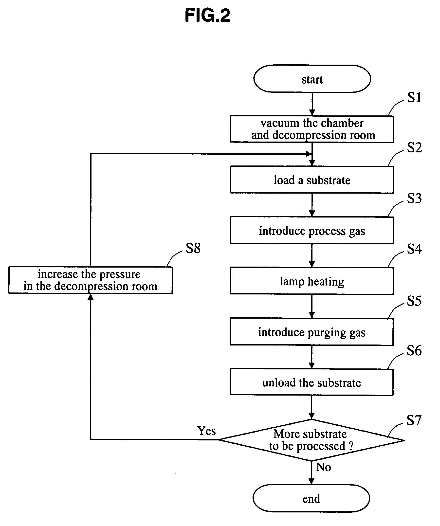
[0035]An embodiment of the present invention is described in detail hereafter with reference to the drawings. In the embodiment below, the present invention is realized in forming an oxide film on the surface of a silicon substrate by ISSG oxidization.

[0036]FIG. 1 is a cross-sectional view showing the structure of a substrate processing apparatus in an embodiment of the present invention. In FIG. 1, the same components as in the prior art substrate processing apparatus shown in FIG. 5 are given the same reference numbers and their explanation is omitted in the detailed explanation below.

[0037]As shown in FIG. 1, a substrate processing apparatus 1 of this embodiment comprises a lamp unit 2 in which multiple lamps such as tungsten halogen lamps are arranged in one plane above a cylindrical chamber 3 in which the substrate is processed via a window assembly 4 as in the prior art substrate processing apparatus 100.

[0038]The chamber 3 is provided with a gas inlet 11 on a sidewall and a g...


PUM

PropertyMeasurementUnit
partial pressuresaaaaaaaaaa
thicknessesaaaaaaaaaa

Abstract

An apparatus for processing a substrate according to the present invention comprises a lamp unit heating the substrate placed in the chamber at a position facing the substrate. A transmission window constituting the top wall of the chamber and transmitting light emitted from the lamp unit is provided between the chamber and the lamp unit. A window assembly having a wall constituted by the transmission window is provided at the lamp unit side of the transmission window. An evacuation unit is connected to the window assembly. A pressure control unit controls the evacuation unit to maintain the internal pressure of the window assembly at a specific pressure. In this way, multiple substrates are subject to a significantly uniform substrate processing when they are processed in succession.

Description

CROSS-REFERENCE TO RELATED APPLICATION[0001]The present application claims the benefit of patent application number 2006-219278, filed in Japan on Aug. 11, 2006, the subject matter of which is incorporated herein by reference.BACKGROUND OF THE INVENTION[0002]1. Field of the Invention[0003]The present invention relates to an apparatus and method for processing a substrate under lamp heating.[0004]2. Description of the Related Art[0005]As finer element patterns have come to be recently used to constitute semiconductor devices, it has been necessary to form thin gate insulating films or shallow impurity diffusion regions in a uniform and stable manner without reducing throughput. Therefore, substrate processing apparatuses of the RTP (rapid thermal process) type are used in the semiconductor device production process, in which short-time thermal processing is performed in a single-wafer process. Among such substrate processing apparatuses, a lamp RTP apparatus has been developed and ex...

Claims


Application Information

Patent Timeline
Patent Type & Authority Applications(United States)
IPC IPC(8): B05D3/06C23C14/00
CPCH01L21/67115H01L21/67253H01L21/67248H01L21/02H01L21/324
Inventor ORIHARA, YASUAKI
Owner PANASONIC CORP
Why Eureka
Try Eureka