Electronic part manufacturing method and base sheet

a manufacturing method and electronic part technology, applied in the direction of printed circuit manufacturing, non-metallic protective coating application, conductive pattern formation, etc., can solve the problem of not controlling unable to make the overall thickness of the layer uniform, and no consideration of the control of the overall thickness of the layer, etc. problem, to achieve the effect of reducing the amount of resin, preventing a large amount of resin, and increasing the flow resistance of resin

Active Publication Date: 2006-11-16
TDK CORPARATION
View PDF2 Cites 1 Cited by
  • Summary
  • Abstract
  • Description
  • Claims
  • Application Information

AI Technical Summary

Benefits of technology

[0025] In the above described structure, after the wiring pattern is formed on the substrate sheet, the insulating sheet is attached to said wiring pattern from above. After the insulating sheet is attached, the temperature of the pressing plate disposed on the rear side of the insulating sheet is increased to heat the insulating sheet. By applying pressure by said pressing plate while applying heat, the conductor portion is caused to penetrate into the resin of the insulating sheet. After the columnar conductor is taken into the interior of the insulating sheet by continuous application of pressure and heat, pressure application is stopped at a certain position. Thus, it is possible to ensure a specific layer thickness in accordance with the position at which pressure application is stopped.
[0026] According to the other more specific structure, after the conductor portion composed of the wiring pattern and the columnar conductor is formed to produce the structure of the substrate sheet, the insulating sheet is attached to the wiring pattern and the columnar conductor from above. After the insulating sheet is attached, the temperature of the pressing plate disposed on the rear side of the insulating sheet is increased to heat the insulating sheet. By applying pressure by said pressure plate while applying heat, the conductor portion is caused to penetrate into the resin of the insulating sheet. As the columnar conductor is taken into the interior of the insulating sheet by continuous application of pressure and heat, the top portion of the columnar conductor comes in contact with the pressing side surface of the insulating sheet. Pressure and heat application is stopped in the state in which the top portion of the columnar conductor is in contact with the pressing side surface of the insulating sheet as above, wherein the columnar conductor function as a stopper. Thus, the thickness of the insulating sheet (or the insulating layer) becomes equal to the height of the columnar conductor, and it is possible to ensure a specific layer thickness.
[0027] Since the resin in the aforementioned insulating sheet has fluidity when heated, when heat and pressure are applied to the insulating film, said resin fills stepped portions and gaps around the wiring pattern and the columnar portion, and the resin tends to extend outwardly from the part formation area. However, since the projecting portion is formed outside the part formation area, flow resistance of the resin increases when the resin reaches the projecting portion. Therefore, it is possible to reduce the amount of the resin that moves outwardly beyond the boundary of the projecting portion (when pressure and heat are applied).
[0028] In view of this, the volume taken up by said conductor portion and said projecting portion within a domain including the projecting portion is firstly computed, and then based on a value thus obtained, the amount of resin for forming a new layer covering said conductor portion is computed. After that, the thickness of the insulating sheet is determined based on the resin amount thus computed. Thus, it is possible to prevent a large amount of resin from flowing out of the domain including the projecting portion and to cover the domain including the projecting portion with the minimum necessary resin amount. By the above process, it is possible to minimize the surplus resin around the conductor portion and to achieve a reduction in the resin consumption. In addition, since it is possible to determine the resin amount appropriately, it is possible to eliminate unevenness of the resin that might occur upon pressing if there is surplus resin, or it is possible to prevent detachment between layers that might be caused if the resin is insufficient.
[0029] The projecting portion and the conductor portion may be formed by the same process step. In that case, it is not necessary to form the conductor portion and the projecting portion by separate process steps, and therefore, it is possible to simplify the process. Moreover, since the projecting portion and the columnar conductor have the same height, when the insulating sheet is pressed while applying heat, it is possible to form a uniform layer without inclination of the sheet between the projecting portion and the columnar conductor. A plurality of electronic parts may be manufactured from the part formation area. Thus, it is possible to manufacture a large number of electronic parts while reducing the consumption amount of the resin.

Problems solved by technology

Nevertheless, in the above-mentioned manufacturing method shown in FIG. 5A, a conductor portion is simply formed in a hole 2 that has been formed on an insulating layer 1 by a laser processing, but the overall thickness of the layer is not controlled.
However, undulation is created on the surface of the insulating resin in accordance with presence / absence of the conductor portions 4, and therefore it is difficult to make the overall thickness of the layer uniform.
Furthermore, in the method in which a bump of electrically conductive paste is formed on wiring on a board and then the bump is caused to penetrate a molded resin by pressing, no consideration has been made on control of the overall thickness of the layer.
However, there is a risk that an external force will act on the surface of the insulating layer in this removing operation and deformation etc. may occur on the surface of the insulating layer.
In addition, since resin is applied to cover conductor portions as with the process shown in FIG. 5B, there is a risk that undulation will be created on the surface of the insulating resin and it will be difficult to make the overall thickness of the layer.
In the technology disclosed in Japanese Patent Application Laid-Open No. 2001-177237 also, an external force acts on the thermosetting insulating resin layer when the PET film is removed, and therefore, there is a risk that deformation may be created on the surface of the thermosetting insulating resin layer, as with the technology disclosed in the above-mentioned patent document.
Accordingly, it might be difficult to make the overall thickness of the layer uniform.
In the method of setting the thickness of a layer by inserting a spacer as disclosed in Japanese Patent Application Laid-Open No. 11-261198, although it is possible to set the layer thickness, it is difficult to achieve connection between layers by a conductor portion at a predetermined position.

Method used


Image

  • Electronic part manufacturing method and base sheet
  • Electronic part manufacturing method and base sheet
  • Electronic part manufacturing method and base sheet

Examples


Embodiment Construction

[0035] In the following, a preferred embodiment of a method for manufacturing an electronic part and a substrate sheet according to the present invention will be described with reference to the drawings.

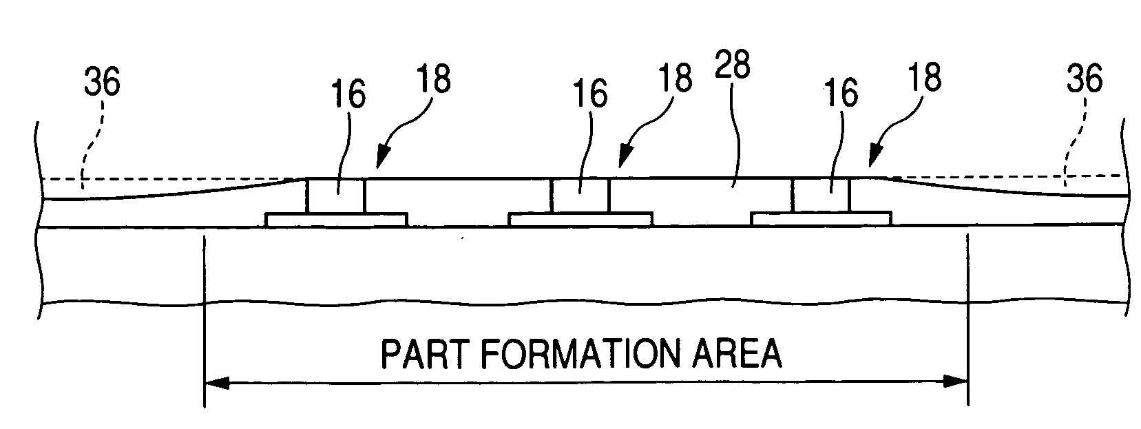
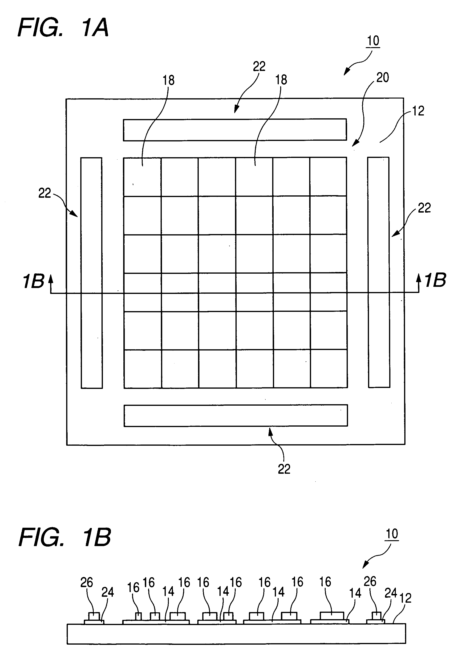
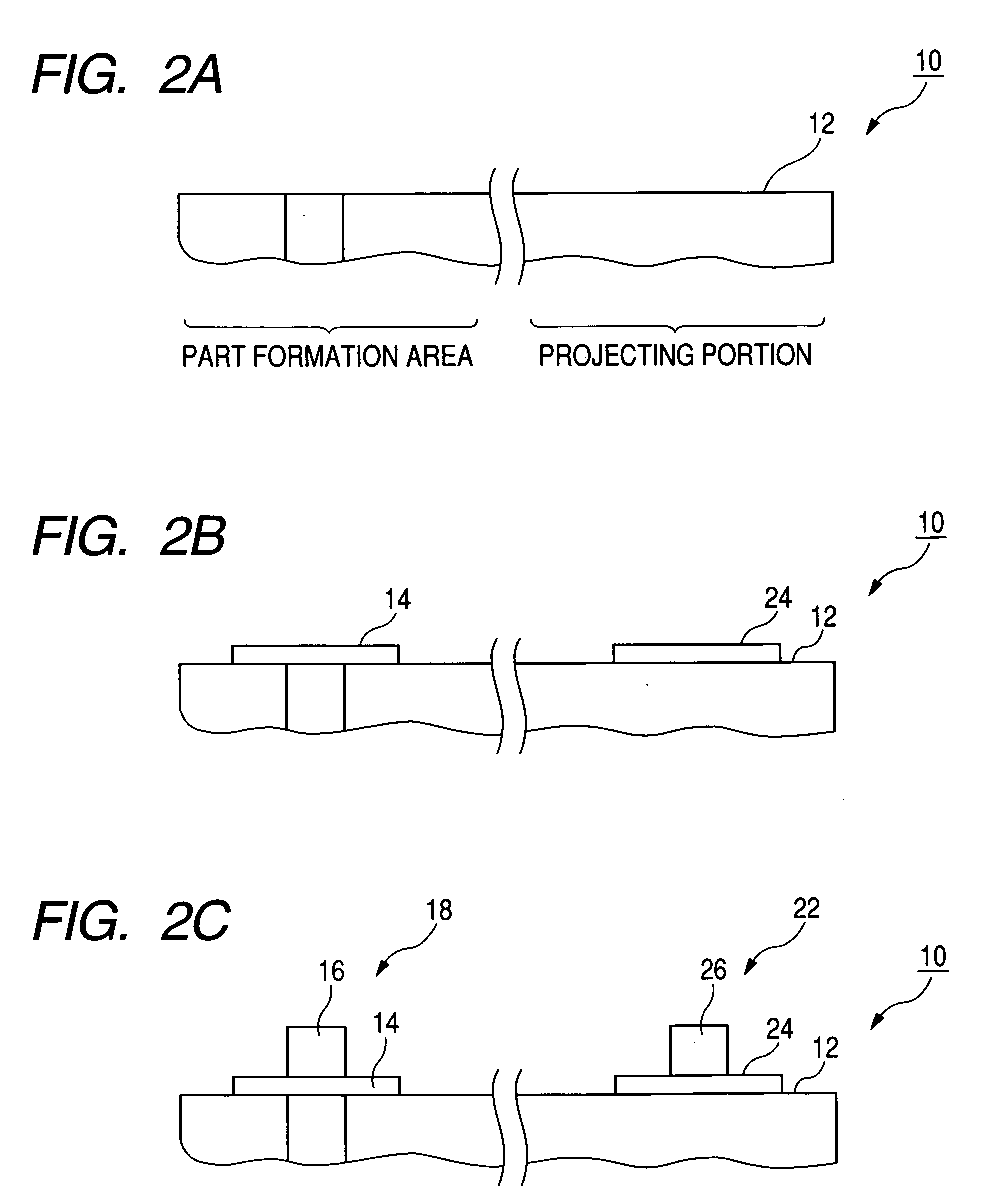
[0036]FIGS. 1A and 1B illustrate a substrate sheet according to an embodiment. FIG. 1A is a plan view, and FIG. 1B is a cross sectional view taken along line 1B-1B in FIG. 1A. As shown in these drawings, wiring patterns 14 and columnar conductors 16 (so-called posts) serving as interlayer connecting portions are formed on a surface of the substrate sheet 10 according to this embodiment. The wiring patterns 14 and the columnar conductors 16 constitute conductor portions 18.

[0037] A part formation area 20 is set in the central portion of the substrate sheet 10, and the plurality of conductor portions 18 mentioned above are formed in this part formation area so that a plurality of electronic parts are to be to be produced therein.

[0038] Outside the part formation area 20 on the subst...


PUM

PropertyMeasurementUnit
thicknessaaaaaaaaaa
flow resistanceaaaaaaaaaa
electrically conductiveaaaaaaaaaa

Abstract

An insulating sheet including resin is attached to a conductor portion composed of a wiring pattern and a columnar conductor from above. Then pressure and heat are applied to the insulating sheet using the columnar conductor as a stopper to form a layer of resin having a uniform thickness with the height of the columnar conductor being a reference to cover the conductor portion. In such method for manufacturing an electronic part, a projecting portion is formed outside a part formation area. In this substrate sheet, the amount of the resin required for forming the layer is computed based on the proportion of the volume taken up by the conductor portion in a domain including the projecting portion, and the thickness of the insulating sheet is set in accordance with the computed resin amount.

Description

TECHNICAL FIELD [0001] The present invention relates to a method for manufacturing an electronic part and to a substrate sheet, and particularly to a method for manufacturing an electronic part in which an electrode portion including a wiring pattern etc. is covered with resin, and to a substrate sheet. BACKGROUND ART [0002] Heretofore, an electronic part and a printed wiring board that have a multilayer structure produced by forming a wiring pattern on an insulating layer and stacking wiring patterns thus formed along their thickness direction have been known. [0003] Various methods of producing such a structure have been proposed and disclosed. FIGS. 5A and 5B are diagrams illustrating steps in a conventional process of producing each layer of an electronic part. [0004] In the step shown in FIG. 5A, a surface of an insulating layer 1 is perforated by irradiation with a layer beam. After a hole 2 is formed by the laser processing, the hole is filled with an electrically conductive ...

Claims


Application Information

Patent Timeline
Patent Type & Authority Applications(United States)
IPC IPC(8): H01L21/00H05K3/28H05K1/02H05K3/46
CPCH05K3/4647H05K2203/066H05K2203/1189Y10T29/49155Y10T29/49126Y10T29/49128Y10T29/49158H05K3/28
Inventor GOTOH, MASASHIKAWASAKI, KAORUYAMAMOTO, HIROSHINAKANO, MUTSUKOKUWAJIMA, HAJIME
Owner TDK CORPARATION
Why Eureka
Try Eureka