Systems and methods for forming metal oxides using metal compounds containing aminosilane ligands

a technology of metal oxides and metal compounds, which is applied in the direction of coatings, capacitors, chemical vapor deposition coatings, etc., can solve the problems of reducing the effective performance of the layer as an insulator, and the performance limits of traditional integrated circuit technology, so as to minimize the detrimental gas phase reaction and improve the control of the thickness of the layer

Inactive Publication Date: 2006-11-16
MICRON TECH INC
View PDF57 Cites 90 Cited by
  • Summary
  • Abstract
  • Description
  • Claims
  • Application Information

AI Technical Summary

Benefits of technology

[0020]“Atomic layer deposition” (ALD) as used herein refers to a vapor deposition process in which numerous consecutive deposition cycles are conducted in a deposition chamber. Typically, during each cycle the metal precursor is chemisorbed to the substrate surface; excess precursor is purged out; a subsequent precursor and / or reaction gas is introduced to react with the chemisorbed layer; and excess reaction gas (if used) and by-products are removed. As compared to the one cycle chemical vapor deposition (CVD) process, the longer duration multi-cycle ALD process allows for improved control of layer thickness by self-limiting layer growth and minimizing detrimental gas phase reactions by separation of the reaction components. The term “atomic layer deposition” as used herein is also meant to include the related terms “atomic layer epitaxy” (ALE), molecular beam epitaxy (MBE), gas source MBE, organometallic MBE, and chemical beam epitaxy when performed with alternating pulses of precursor compound(s), reaction gas(es), and purge (i.e., inert carrier) gas.

Problems solved by technology

The continuous shrinkage of microelectronic devices such as capacitors and gates over the years has led to a situation where the materials traditionally used in integrated circuit technology are approaching their performance limits.
However, when the SiO2 layer is thinned to 1 nm (i.e., a thickness of only 4 or 5 molecules), as is desired in the newest micro devices, the layer no longer effectively performs as an insulator due to the tunneling current running through it.

Method used


Image

  • Systems and methods for forming metal oxides using metal compounds containing aminosilane ligands
  • Systems and methods for forming metal oxides using metal compounds containing aminosilane ligands
  • Systems and methods for forming metal oxides using metal compounds containing aminosilane ligands

Examples


example

Example 1

Deposition of Y2O3 by Atomic Layer Deposition

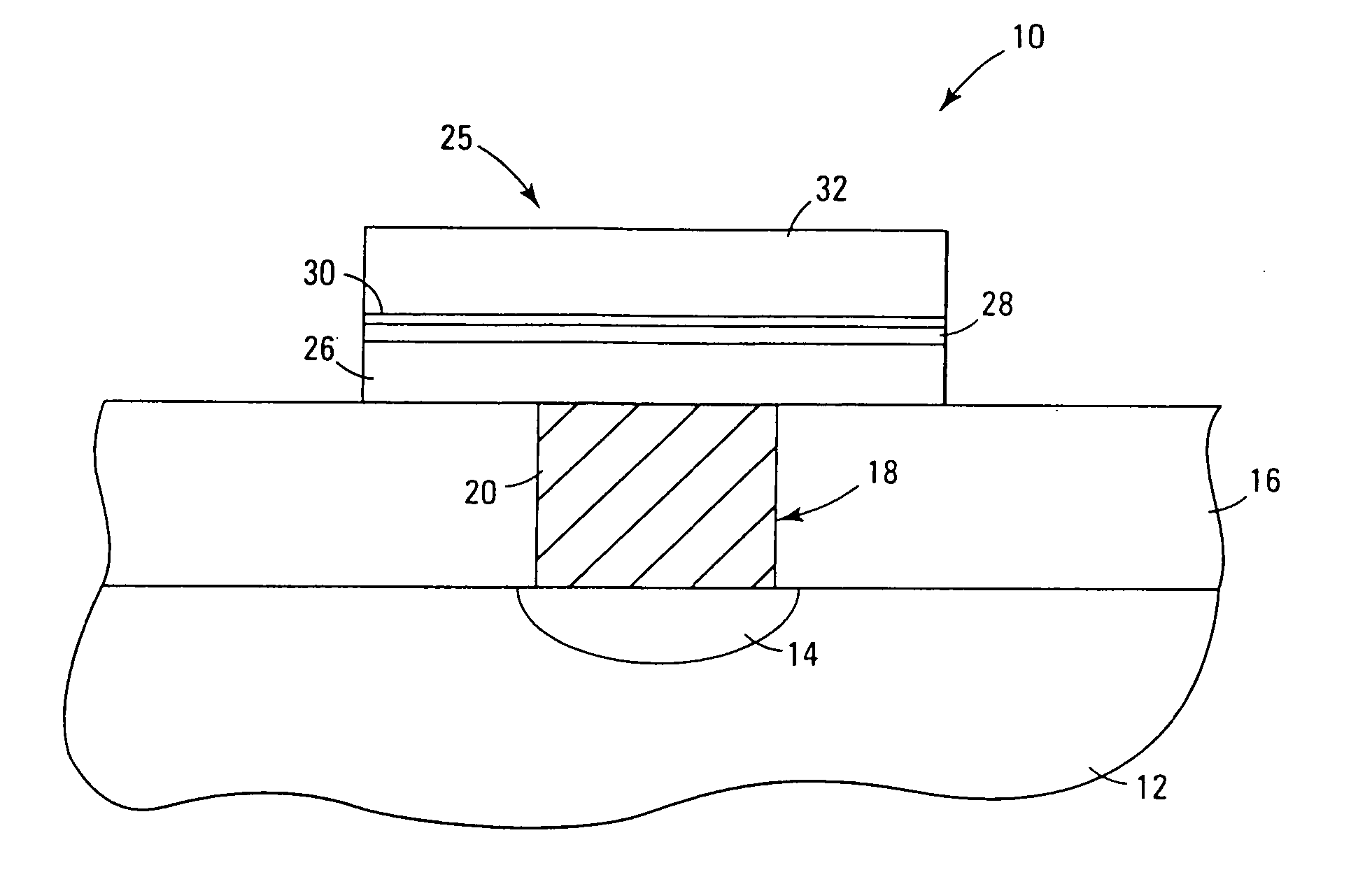
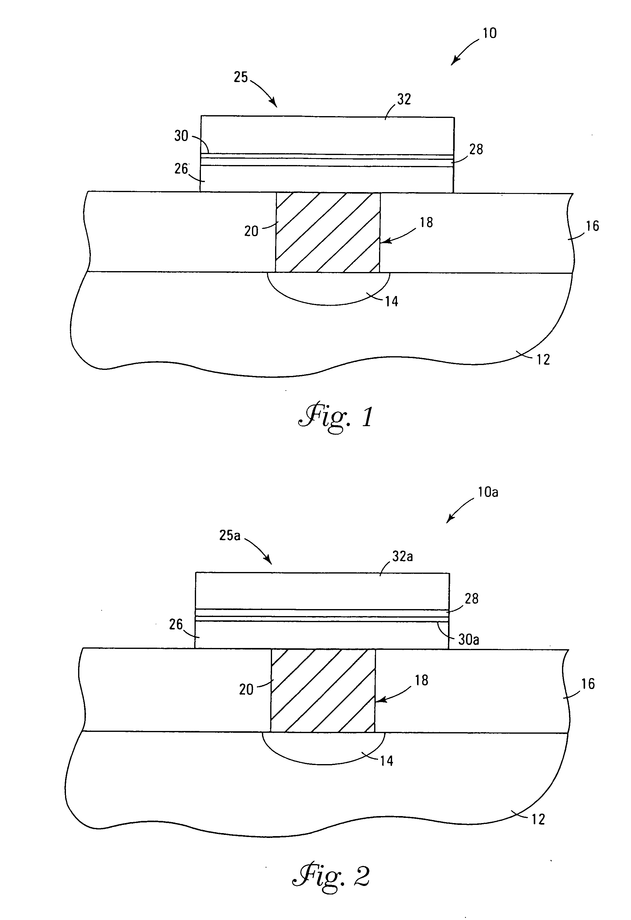
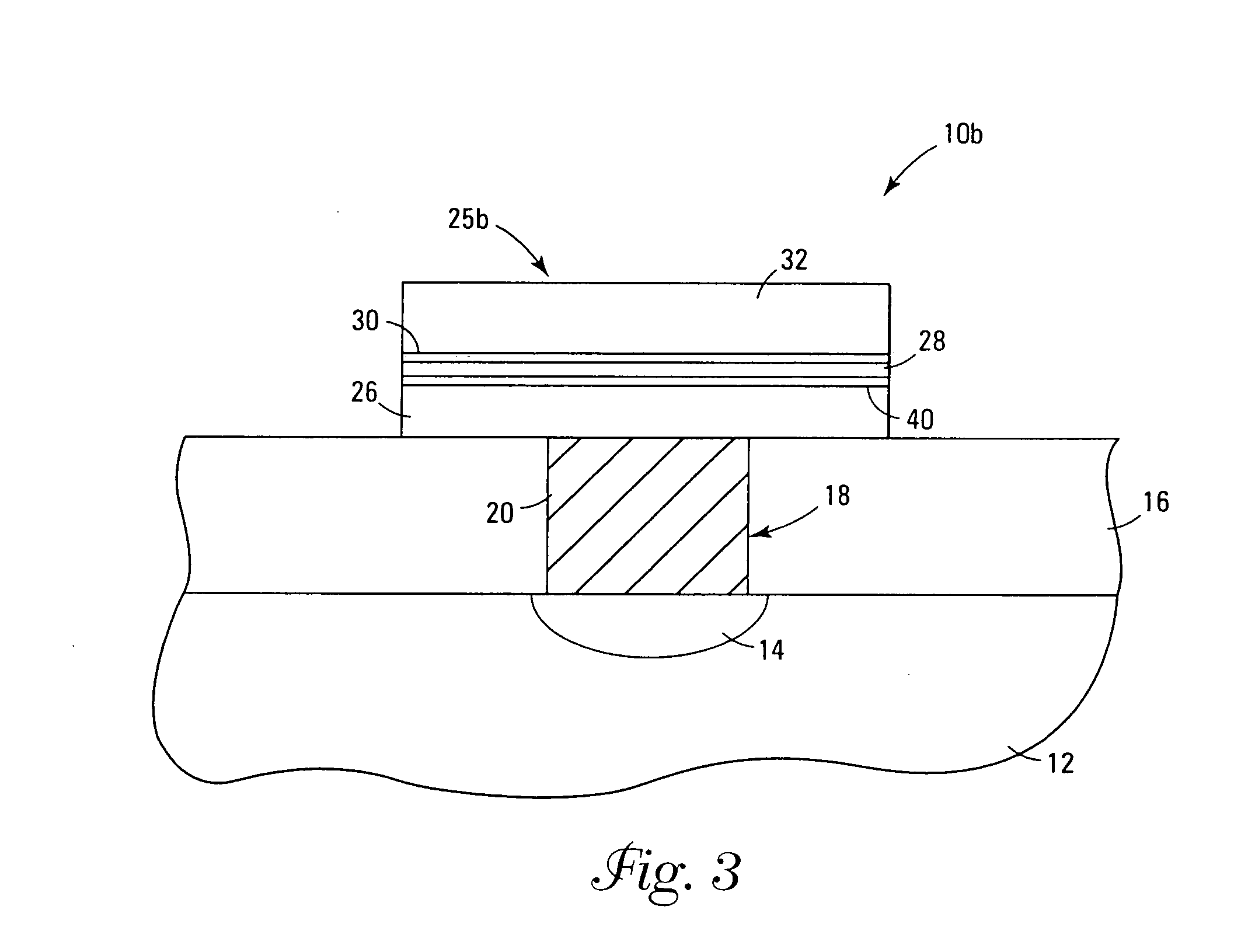
[0070] A Y2O3 film was deposited on a 100 nm PVD Pt bottom electrode by ALD using alternate pulses of Y[N(tBu)Si(H)(Me)2]3 and water; at a substrate temperature of 298° C. A 1000 Å film resulted from 750 cycles. Each cycle consisted of a 1 s yttrium dose, 5 s vacuum pump, 0.75 s water dose, is argon purge, 5 s vacuum pump. A flat capacitor test structure of sputtered Pt top electrodes on top of the Y2O3 was used to measure the electrical data. Several of the capacitors had measured dielectric constants near 30 (0.1-100 kHz) and leakage between 10−7 and 10−8 A / cm2 at 1 V after 700° C. RTO. XPS analysis revealed that carbon was below detection limits after the oxidation anneal but 16 atom % Si remained in the Y2O3 layer.


PUM

PropertyMeasurementUnit
thicknessaaaaaaaaaa
adsorption energiesaaaaaaaaaa
pressureaaaaaaaaaa

Abstract

A method of forming (and an apparatus for forming) a metal oxide layer on a substrate, particularly a semiconductor substrate or substrate assembly, using a vapor deposition process and one or more precursor compounds that include aminosilane ligands.

Description

[0001] This is a divisional of application Ser. No. 10 / 229,841, filed Aug. 28, 2002, (pending), which is incorporated herein by reference in its entirety.FIELD OF THE INVENTION [0002] This invention relates to methods of forming a metal oxide layer on a substrate using one or more precursor compounds that include one or more aminosilane ligands during a vapor deposition process. The precursor compounds and methods are particularly suitable for the formation of metal oxide layers on semiconductor substrates or substrate assemblies. BACKGROUND OF THE INVENTION [0003] The continuous shrinkage of microelectronic devices such as capacitors and gates over the years has led to a situation where the materials traditionally used in integrated circuit technology are approaching their performance limits. Silicon (i.e., doped polysilicon) has generally been the substrate of choice, and silicon dioxide (SiO2) has frequently been used as the dielectric material with silicon to construct microelec...

Claims


Application Information

Patent Timeline
Patent Type & Authority Applications(United States)
IPC IPC(8): H01L21/473C23C16/00C23C16/40C23C16/44C23C16/455H01L21/02H01L21/316H01L21/8242
CPCC23C16/405C23C16/45553H01L28/40H01L21/31683H01L21/31604H01L21/02194H01L21/02205H01L21/02183H01L21/02271H01L21/0228
Inventor VAARTSTRA, BRIAN A.QUICK, TIMOTHY A.
Owner MICRON TECH INC
Why Eureka
Try Eureka