Method for patterning on a wafer having at least one substrate for the realization of an integrated circuit

a technology of integrated circuits and substrates, which is applied in the direction of decorative surface effects, decorative arts, instruments, etc., can solve the problems of not always being able to detect a typical emission band in correspondence with the end point, and the etching step is difficult to detect a predetermined end point, so as to achieve useful indications of the reaction

Inactive Publication Date: 2006-11-23
STMICROELECTRONICS SRL
View PDF18 Cites 6 Cited by
  • Summary
  • Abstract
  • Description
  • Claims
  • Application Information

AI Technical Summary

Benefits of technology

[0034] A result of this further embodiment is that from the IR signal it is possible to unequivocally determine the chemical nature of the molecular ...

Problems solved by technology

A problem associated to the reactive gas plasma etching method is the difficulty to detect a predetermined end point of the etching step, e.g., the moment when a predetermined amount, or a whole substrate has been removed, thereby obtaining a full substrate etching.
Nevertheless, it is not always possible to detect a typical emission band in correspondence with the end point.
In particular, some reactive gas plasmas being presently used do not allow a significant intensity variation of the emission signal to be detected.
This last method has, however, the drawback to require each time the definition of new etching process parameters both from the morphological point of view and from the electric point of view.
This method has, however, the...

Method used


Image

  • Method for patterning on a wafer having at least one substrate for the realization of an integrated circuit
  • Method for patterning on a wafer having at least one substrate for the realization of an integrated circuit
  • Method for patterning on a wafer having at least one substrate for the realization of an integrated circuit

Examples


Embodiment Construction

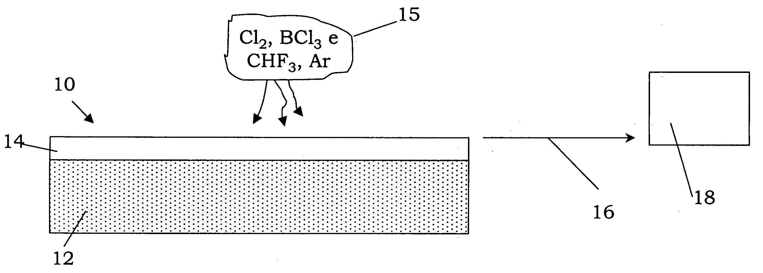
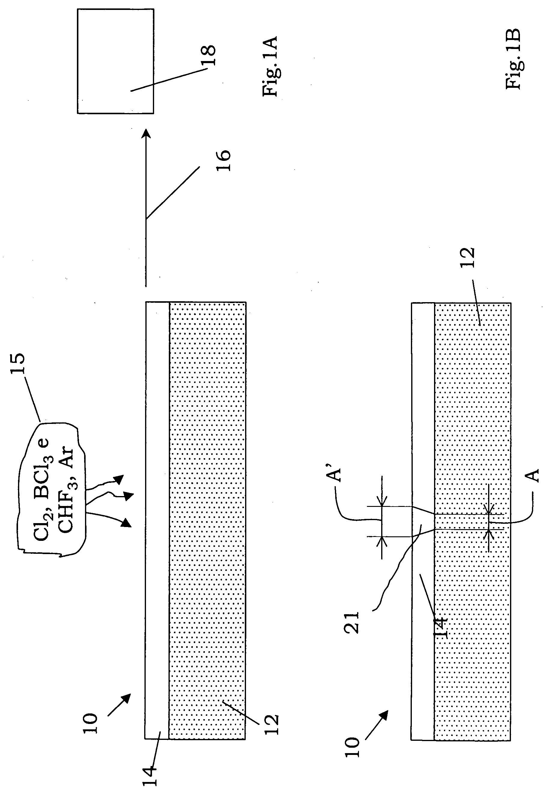
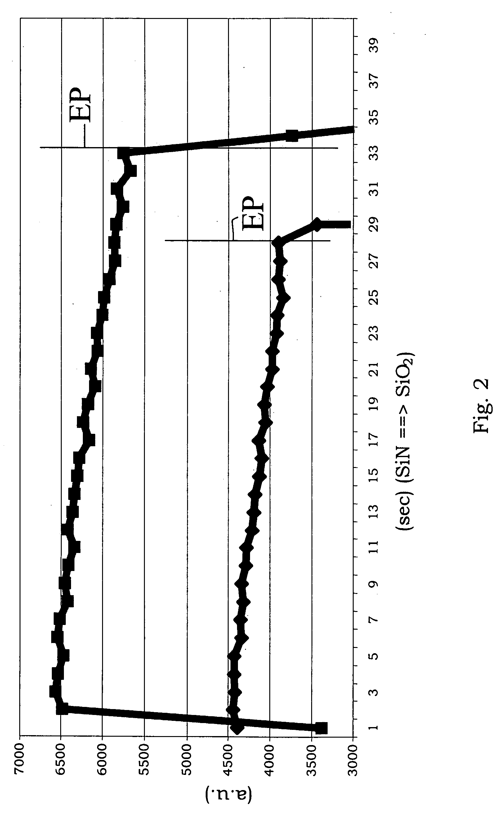
[0045] Embodiments of a method for patterning on a wafer having at least one substrate for the realization of an integrated circuit are described herein. In the following description, numerous specific details are given to provide a thorough understanding of embodiments. One skilled in the relevant art will recognize, however, that the invention can be practiced without one or more of the specific details, or with other methods, components, materials, etc. In other instances, well-known structures, materials, or operations are not shown or described in detail to avoid obscuring aspects of the invention.

[0046] Reference throughout this specification to “one embodiment” or “an embodiment” means that a particular feature, structure, or characteristic described in connection with the embodiment is included in at least one embodiment. Thus, the appearances of the phrases “in one embodiment” or “in an embodiment” in various places throughout this specification are not necessarily all ref...


PUM

PropertyMeasurementUnit
Fractionaaaaaaaaaa
Fractionaaaaaaaaaa
Fractionaaaaaaaaaa

Abstract

A method is provided for patterning a wafer comprising at least one substrate for the manufacture of an integrated circuit. The method comprises: etching at least one portion of the substrate with a reactive gas plasma to obtain an optical emission signal, resulting from the products of the reaction between the plasma and the substrate and having a predetermined spectral fingerprint; carrying on the etching of the substrate up to a predetermined end point; and monitoring the spectral fingerprint of the optical emission signal to detect the etching end point. The method comprises the further insertion of an inert gas in the plasma to obtain an increase in the intensity of the optical emission signal.

Description

TECHNICAL FIELD [0001] The present disclosure relates in its more general aspect to the manufacture of electronic semiconductor devices, and more particularly but not exclusively to a method for patterning a wafer comprising at least one substrate for the manufacture of an integrated circuit. [0002] In its even more particular but not exclusive aspects, the method comprises: [0003] etching at least one substrate portion with a reactive gas plasma obtaining an optical emission signal resulting from the products of a reaction between the plasma and the substrate and having a predetermined spectral fingerprint, [0004] carrying on the etching of the at least one substrate portion up to a predetermined end point, and [0005] monitoring the spectral fingerprint of the optical emission signal to detect this end point of the etching. BACKGROUND INFORMATION [0006] The manufacture of electronic semiconductor devices is performed by exposing silicon wafers to a series of chemical-physical treat...

Claims


Application Information

Patent Timeline
IPC IPC(8): G01L21/30H01L21/302C23F1/00B44C1/22
CPCH01L21/31116
Inventor FAZIO, GIUSEPPESPANDRE, ALESSANDROPETRUZZA, PIETRO
Owner STMICROELECTRONICS SRL
Why Eureka
Try Eureka