Semiconductor device and photoelectric conversion device and scanner using the same

a technology of photoelectric conversion and semiconductor chip, applied in solid-state devices, basic electric elements, television systems, etc., can solve the problems of deteriorating image quality of pixel data of that portion shown with white, affecting the performance of the scanner, and affecting the accuracy of the scanner

Inactive Publication Date: 2006-11-23
ROHM CO LTD
View PDF4 Cites 9 Cited by
  • Summary
  • Abstract
  • Description
  • Claims
  • Application Information

AI Technical Summary

Benefits of technology

[0017] An object of the present invention is to retain immunity to electrostatic breakdown and to prevent malfunction due to input of electrostatic noise to a parasitic element in a semiconductor device used for a photoelectric conversion device.
[0034] With the use of the semiconductor device according to the present invention, even if pulsed noise such as electrostatic noise is input to the semiconductor device, turn-on of the parasitic element can be suppressed by fixing a voltage of an impurity region implementing the parasitic element resulted from a vertical structure. Therefore, deterioration in an image such as generation of a lateral line across the image can be suppressed. In addition, without providing one of the diodes that have been connected in an electrically reverse direction to the power supply voltage side and the reference voltage side respectively of a conventional input / output terminal, immunity to electrostatic breakdown can be improved and breakdown of the internal circuit due to electrostatic noise can be suppressed by providing a diode connected in an electrically reverse direction between the reference voltage and the power supply voltage.

Problems solved by technology

Application of excessive pulsed electrostatic noise to the semiconductor chip may result in breakdown of an internal circuit of the semiconductor chip.
For example, if electrostatic noise is applied during reading of a portion that should be read as black (in which case the current does not flow through the photodiode), such image quality deterioration that pixel data of that portion is shown with white is caused.
In general, measures such as mixing of a conductive substance in glass 54 through which the image is read or use of a shield with metal of the glass surface are available as methods for preventing the electrostatic noise, however, it has been difficult to employ such measures for preventing the electrostatic noise, because a component on or above optical signal input means should essentially be clear and colorless.

Method used


Image

  • Semiconductor device and photoelectric conversion device and scanner using the same
  • Semiconductor device and photoelectric conversion device and scanner using the same
  • Semiconductor device and photoelectric conversion device and scanner using the same

Examples


first embodiment

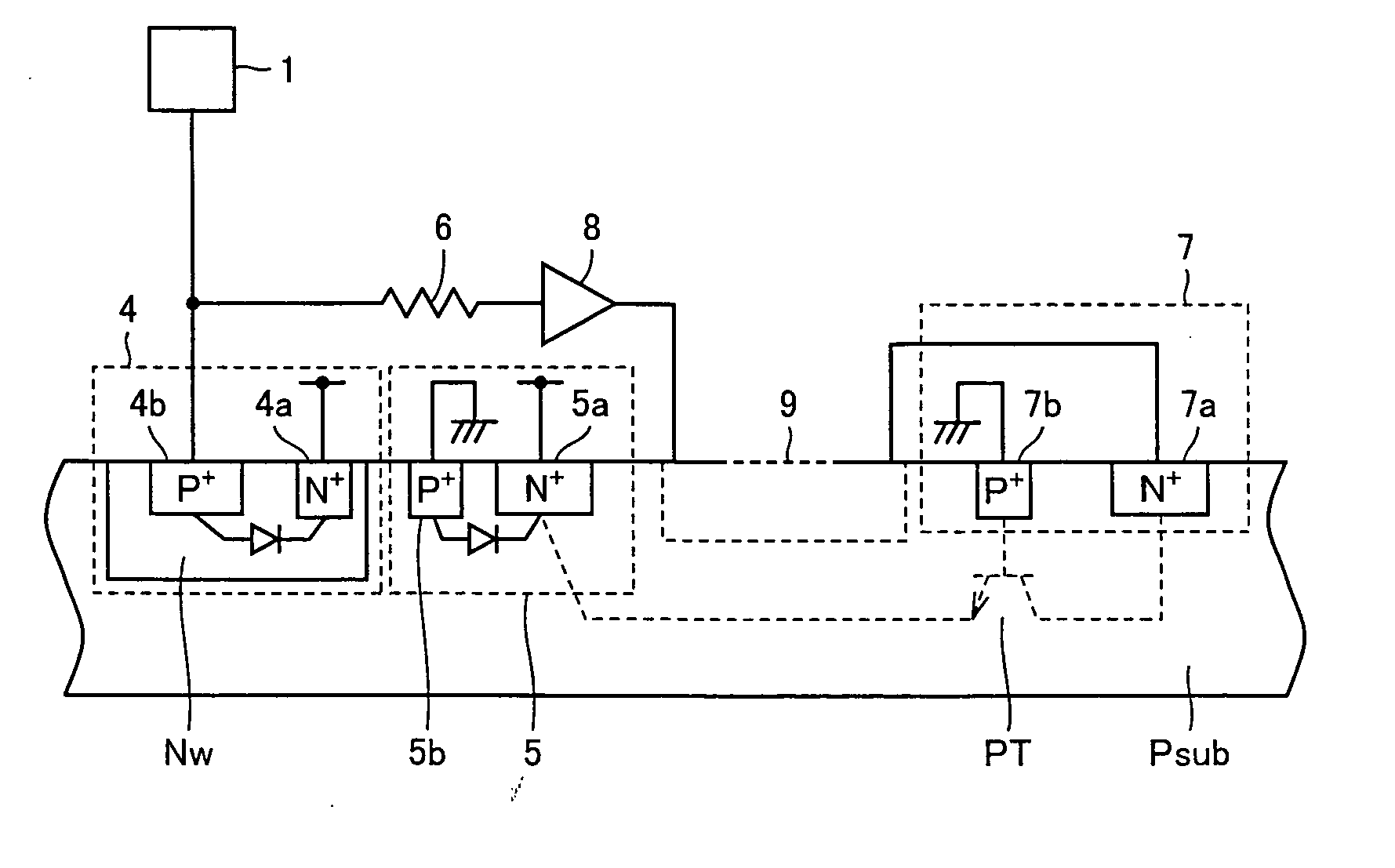
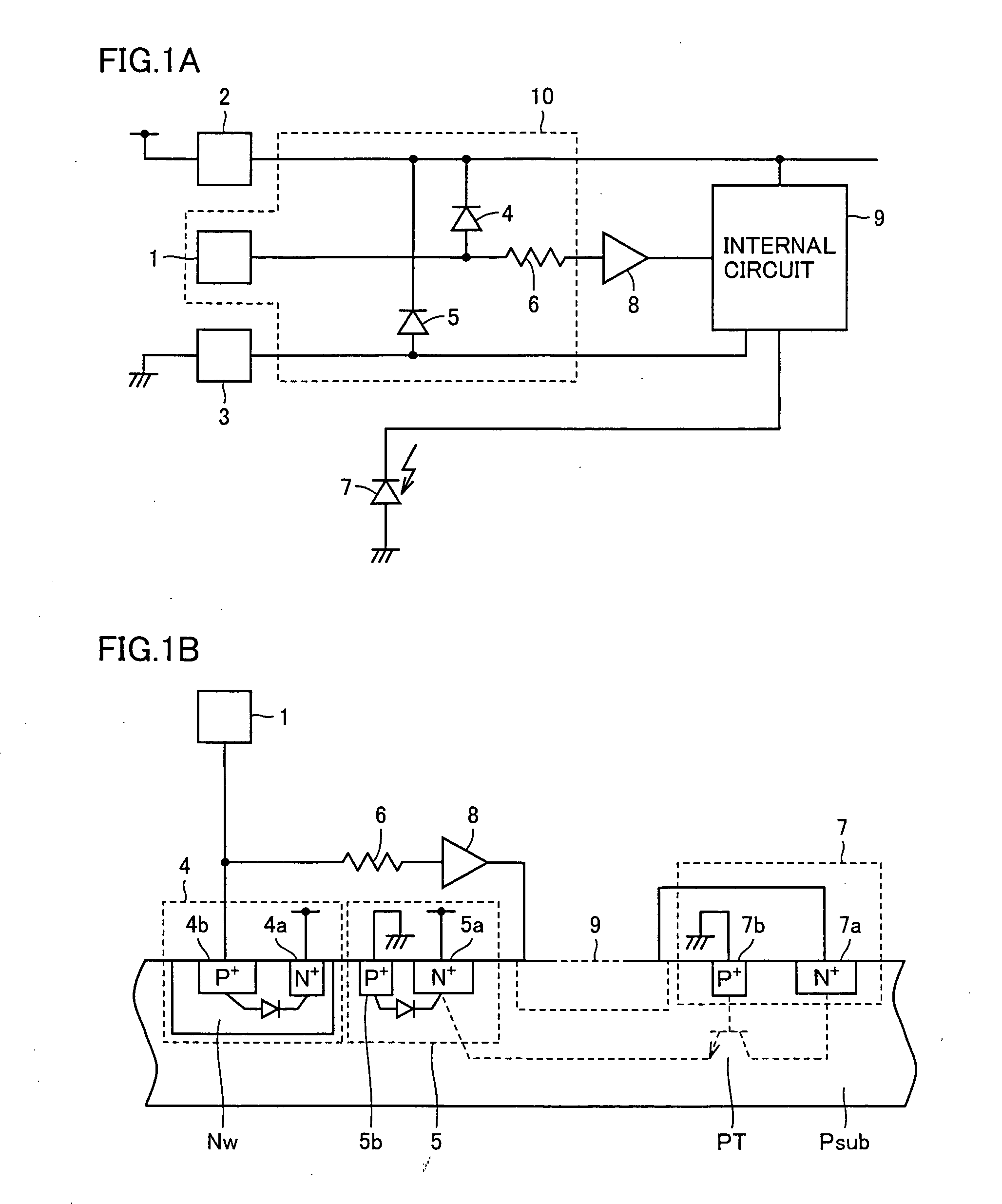
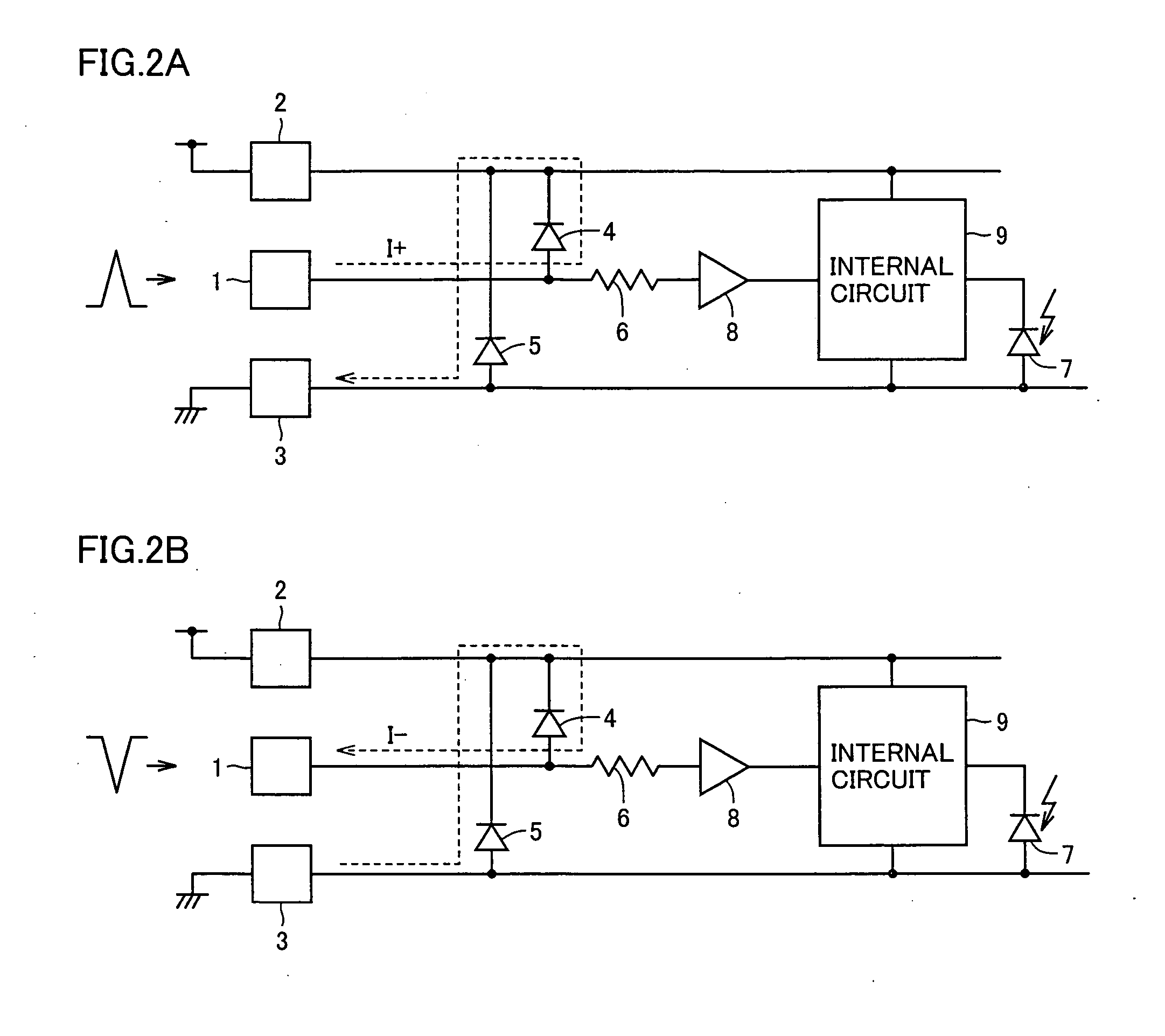
[0047] A configuration of a semiconductor device according to one embodiment of the present invention will be described with reference to FIG. 1A. Semiconductor device 100 according to the present invention includes as terminals, signal terminal 1 receiving a fluctuating electric signal, first voltage terminal 2 receiving, for example, first voltage Vcc as the power supply voltage, and second voltage terminal 3 receiving, for example, second voltage Vss lower than the first voltage as a ground voltage. An electrostatic protection circuit 10 is configured with first protection element 4 having the anode connected to signal terminal 1 and the cathode connected to the first voltage terminal (a diode is shown as an example of the protection element), second protection element 5 having the cathode side connected to the first voltage terminal and the anode side connected to second voltage terminal 3, and a resistor 6 having one end connected to a point of connection of signal terminal 1 a...

second embodiment

[0054] A configuration of semiconductor device 200 according to another embodiment of the present invention will be described with reference to FIG. 3A. Semiconductor device 200 according to the present invention includes as terminals, signal terminal 21 receiving a fluctuating electric signal, first voltage terminal 22 receiving, for example, first voltage Vcc as the power supply voltage, and second voltage terminal 23 receiving, for example, second voltage Vss lower than the first voltage as the ground voltage. An electrostatic protection circuit 20 is configured with first protection element 24 having the cathode connected to signal terminal 21 and the anode connected to second voltage terminal 23, second protection element 25 having the cathode side connected to first voltage terminal 22 and the anode side connected to second voltage terminal 23, and a resistor 26 having one end connected to a point of connection of signal terminal 21 and the cathode of first protection element ...


PUM


Abstract

A semiconductor device includes a photoelectric conversion element outputting an electric signal in accordance with an externally input optical signal, an internal circuit processing the electric signal, a signal terminal inputting or outputting a signal to the internal circuit, a first voltage terminal supplying a first voltage to the internal circuit, and a second voltage terminal supplying a second voltage lower than the first voltage to the internal circuit. The semiconductor device further includes a first protection element connected in an electrically reverse direction between the signal terminal and the first voltage and having at least one PN junction and a second protection element connected in an electrically reverse direction between the first voltage and the second voltage and having at least one PN junction, so that immunity to electrostatic noise can be improved and electrostatic breakdown and malfunction of the photoelectric conversion element can be suppressed.

Description

BACKGROUND OF THE INVENTION [0001] 1. Field of the Invention [0002] The present invention relates to a semiconductor device converting an optical signal to an electric signal, and to a semiconductor device configured to improve immunity to electrostatic breakdown and to prevent malfunction caused by electrostatic noise by arranging a new protection element at a prescribed position as well as to a photoelectric conversion device using the semiconductor device or a scanner using the photoelectric conversion device. [0003] 2. Description of the Background Art [0004] In a scanner reading various image data, for example as shown in FIG. 7, a document is fixed on a glass surface 54 and irradiated with light from below, an image sensor portion 51 reading an image is moved, the light reflected from the document is converted to an electric signal, and the data is transferred to information equipment such as a computer. A flatbed scanner 500 includes image sensor portion 51 reading the image,...

Claims


Application Information

Patent Timeline
Patent Type & Authority Applications(United States)
IPC IPC(8): H01L23/62
CPCH01L27/0255H01L27/14643H04N5/369H04N5/335H01L31/02019H04N25/00H04N25/70
Inventor YAMADA, NOBUYUKITAMAGAWA, TOSHIMITSU
Owner ROHM CO LTD
Why Eureka
Try Eureka