Electroless deposition process on a silicon contact

a silicon contact and electroless technology, applied in the direction of liquid/solution decomposition chemical coating, coating, material nanotechnology, etc., can solve the problems of affecting the device yield of the fabricated substrate, the deposition process for storing these materials, and the displacement of voids from one layer to the nex

Active Publication Date: 2006-11-23
APPLIED MATERIALS INC
View PDF99 Cites 306 Cited by
  • Summary
  • Abstract
  • Description
  • Claims
  • Application Information

AI Technical Summary

Problems solved by technology

Although copper and tungsten are popular interconnect materials, deposition processes for depositing these materials may suffer by forming a void or a seam within the contact plug, as illustrated in FIG. 1C.
Defects, such as a seam or void 114, may cause a series of problems during the fabrication of electronic devices depicted herein.
However, a more serious obstacle during fabrication is the displacement of voids from one layer to the next.
Ultimately, the defects in conductive layer 112 can affect the device yield of the fabricated substrate.

Method used


Image

  • Electroless deposition process on a silicon contact
  • Electroless deposition process on a silicon contact
  • Electroless deposition process on a silicon contact

Examples


Embodiment Construction

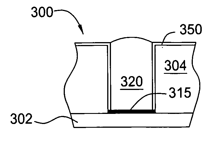
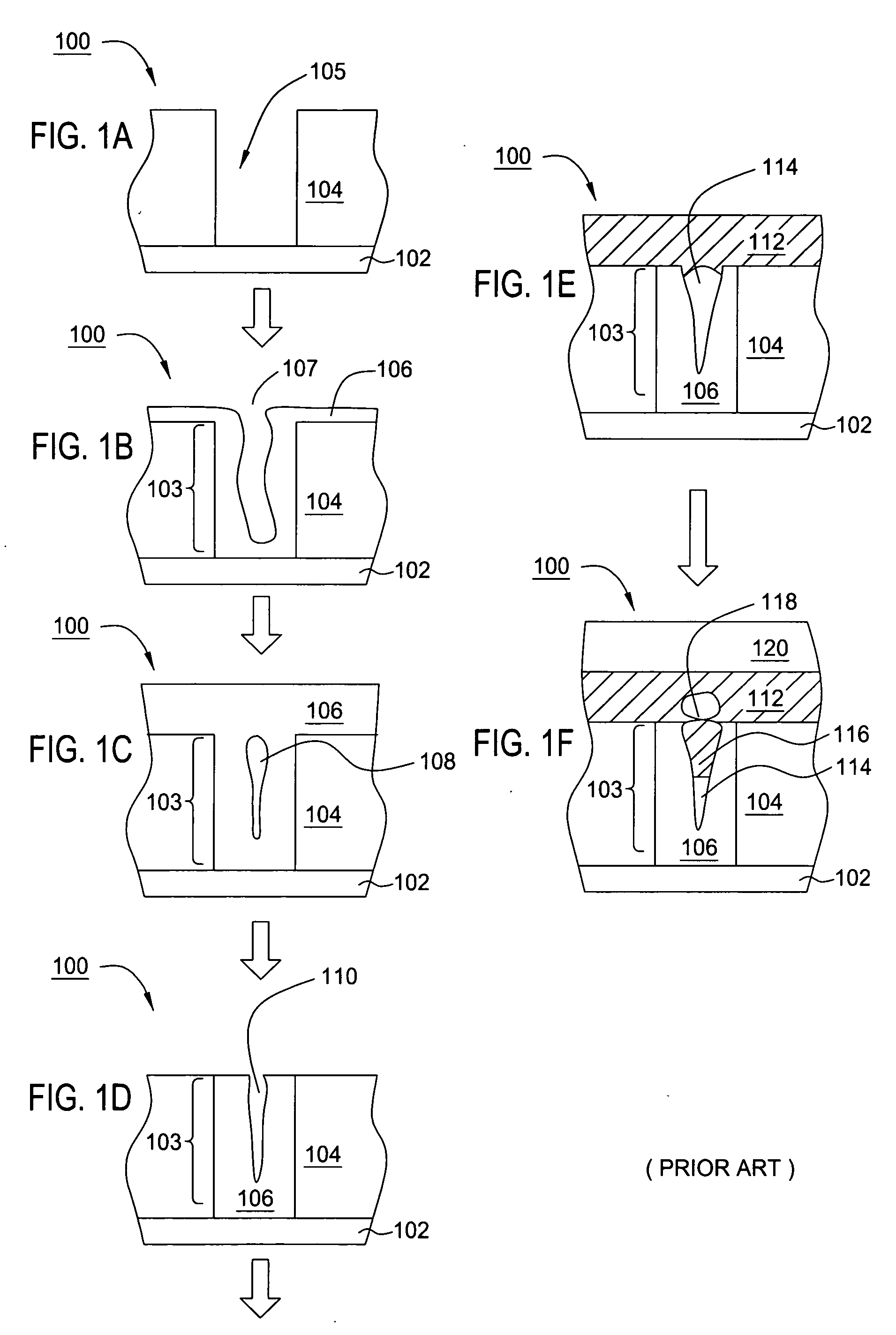
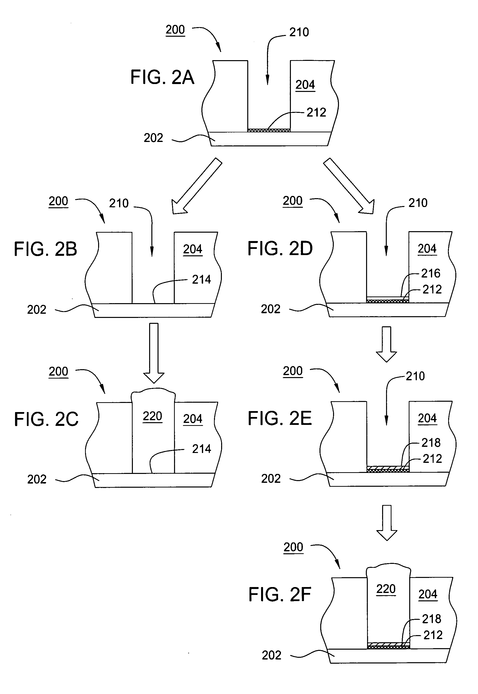
[0033] Embodiments as described herein provide methods for depositing a material on a substrate during electroless deposition processes. In one embodiment, the substrate contains a contact aperture having an exposed silicon contact surface. In another embodiment, the substrate contains a contact aperture having an exposed silicide contact surface. The apertures are filled with a metal contact material by exposing the substrate to an electroless deposition process. The metal contact material may contain a cobalt material, a nickel material, and alloys thereof. Prior to filling the apertures, the substrate may be exposed to a variety of pretreatment processes, such as preclean processes and activations processes. A preclean process may remove organic residues, native oxides, and other contaminants during a wet clean process or a plasma etch process. Embodiments of the process also provide the deposition of additional layers, such as a capping layer.

Metal-Containing Interconnect Proc...


PUM

PropertyMeasurementUnit
molar ratioaaaaaaaaaa
pressureaaaaaaaaaa
pressureaaaaaaaaaa

Abstract

Embodiments as described herein provide methods for depositing a material on a substrate during electroless deposition processes, as well as compositions of the electroless deposition solutions. In one embodiment, the substrate contains a contact aperture having an exposed silicon contact surface. In another embodiment, the substrate contains a contact aperture having an exposed silicide contact surface. The apertures are filled with a metal contact material by exposing the substrate to an electroless deposition process. The metal contact material may contain a cobalt material, a nickel material, or alloys thereof. Prior to filling the apertures, the substrate may be exposed to a variety of pretreatment processes, such as preclean processes and activations processes. A preclean process may remove organic residues, native oxides, and other contaminants during a wet clean process or a plasma etch process. Embodiments of the process also provide the deposition of additional layers, such as a capping layer.

Description

CROSS-REFERENCE TO RELATED APPLICATIONS [0001] This application claims benefit of U.S. Ser. No. 60 / 663,493, filed Mar. 18, 2005 (9916L), U.S. Ser. No. 60 / 683,599, filed May 23, 2005 (9916L.02), U.S. Ser. No. 60 / 703,538, filed Jul. 29, 2005 (9916L.03), U.S. Ser. No. 60 / 703,633, filed Jul. 29, 2005 (9916L.04), U.S. Ser. No. 60 / 709,564, filed Aug. 19, 2005 (9916L.05), U.S. Ser. No. 60 / 754,230, filed Dec. 27, 2005 (9916L.06), and U.S. Ser. No. 60 / 731,624, filed Oct. 28, 2005 (10659L), which are all herein incorporated by reference in their entirety.BACKGROUND OF THE INVENTION [0002] 1. Field of the Invention [0003] Embodiments of the invention generally relate to methods for depositing materials on substrates, and more specifically to methods for filling apertures within a high aspect ratio contact. [0004] 2. Description of the Related Art [0005] Multilevel, 45 nm node metallization is one of the key technologies for the next generation of very large scale integration (VLSI). The multil...

Claims


Application Information

Patent Timeline
Patent Type & Authority Applications(United States)
IPC IPC(8): H01L21/44
CPCB82Y30/00H01L21/76889C23C18/1893C23C18/32C23C18/34H01L21/02063H01L21/28518H01L21/288H01L21/76802H01L21/76814H01L21/76843H01L21/76847H01L21/76855H01L21/76856H01L21/76867H01L21/76874C23C18/1651H01L21/76879
Inventor STEWART, MICHAEL P.WEIDMAN, TIMOTHY W.SHANMUGASUNDRAM, ARULKUMAREAGLESHAM, DAVID J.
Owner APPLIED MATERIALS INC
Why Eureka
Try Eureka