Manufacturing gallium nitride substrates by lateral overgrowth through masks and devices fabricated thereof

a technology of gallium nitride and substrate, which is applied in the direction of crystal growth process, polycrystalline material growth, chemically reactive gas growth, etc., can solve the problems of high defect parts, filtering of defects, and complex lds technology of elo

Active Publication Date: 2006-11-30
IV WORKS
View PDF9 Cites 101 Cited by
  • Summary
  • Abstract
  • Description
  • Claims
  • Application Information

AI Technical Summary

Problems solved by technology

The basic idea is that this technique may lead to a filtering of the defects: above the windows, the microstructure of the underlying GaN template is reproduced, whereas the laterally grown material (over the mask) is defect free.
In this method, however, some parts of the surface remain highly defective (coherent part above the openings and coalescence boundaries).
This makes the technology of LDs on ELO also complicated since device structures have to be fabricated on the good part of the template over layer and thereby the yield of fabrication is low.

Method used


Image

  • Manufacturing gallium nitride substrates by lateral overgrowth through masks and devices fabricated thereof
  • Manufacturing gallium nitride substrates by lateral overgrowth through masks and devices fabricated thereof
  • Manufacturing gallium nitride substrates by lateral overgrowth through masks and devices fabricated thereof

Examples


example 1

A Suitable Epitaxial Growth Reactor is Used for the Metal Organic Vapour Phase Epitaxy.

[0054] [1] Explicitly, a substrate 1, especially (0001) sapphire is used. A very thin film of silicon nitride 2 is formed on the surface of the sapphire, the film being obtained by reaction between NH3 and silane SiH4 for a time short enough to limit the thickness of the film to that of about a few atomic planes.

The operating conditions are the following:

[0055] [2] The gaseous vehicle is a mixture of nitrogen and hydrogen in equal proportions. The ammonia is introduced together with the silane, in a form diluted to 50 ppm in hydrogen. Under these conditions, the typical NH3 and SiH4 reaction time is of the order of 30 seconds.

[0056] The successive steps are monitored by laser reflectometry (LR). After the dielectric layer has been completely formed, a continuous gallium nitride layer having a thickness of 20 to 30 nm is deposited on the dielectric film. The deposition of the GaN layer is mad...

example 2

Shorter or Longer First ELO Process: Void Engineering.

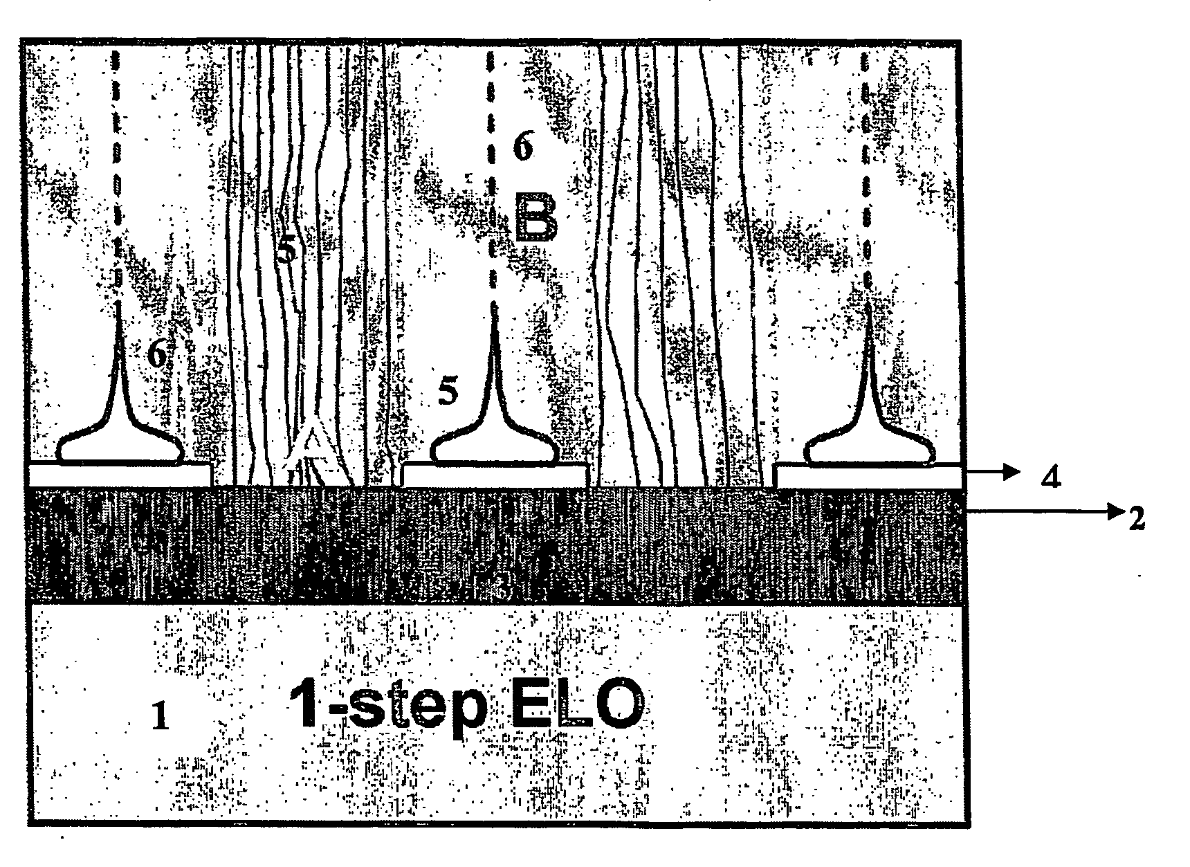
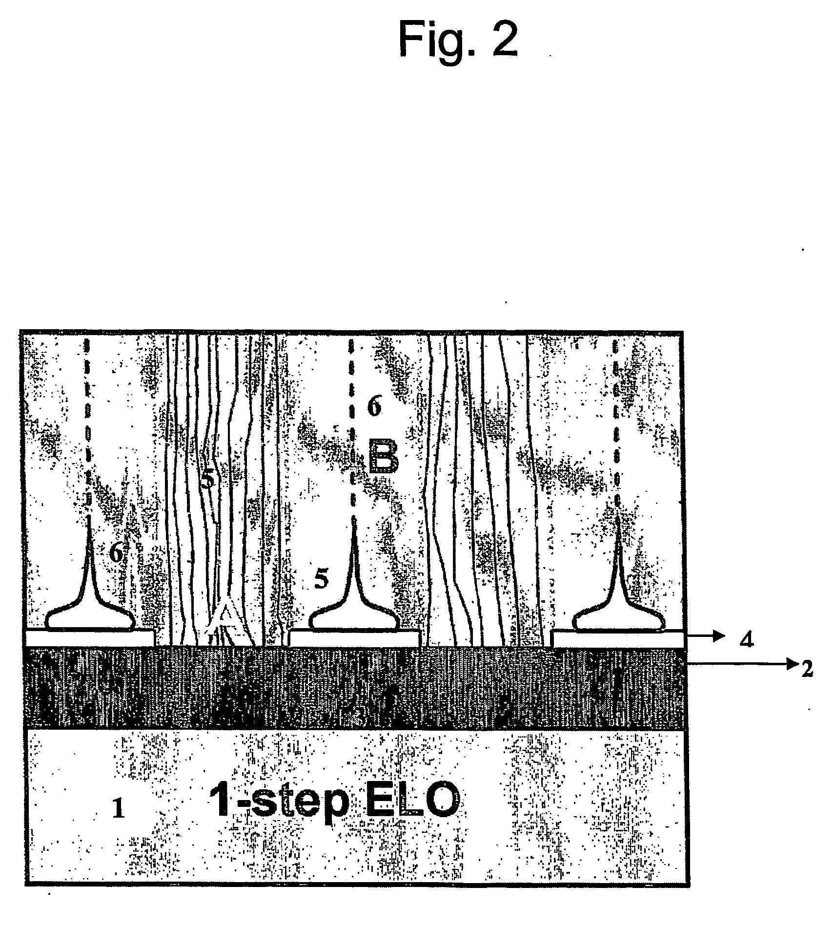
[0062] [1] The example 1 describes a double 2S-ELO GaN in which the two 2S-ELO have basically the same duration. In other modifications of the process the first 2S-ELO could be longer (FIG. 5), in such a way that remaining TDs from the first 2S-ELO starting to be redistributed will be either bent at 90° or stopped by the mask.

[0063] [2] Conversely, the second 2S-ELO can start even before full coalescence, (FIG. 6). In this later modification a void V can be created, and the shape of the void can be tuned from the growing conditions. In FIG. 6, the mask 8 covers partially the (0001) plane and completely the V-Shaped facets. This second alternative of the process described in the example 1 indeed allows controlling the shapes and distributions of voids. Henceforth, this void engineering can be adjusted to favour spontaneous strain induced separation of the upper part 10 from the substrate 1.

[3] Such a process produces GaN with...

example 3

Void Engineering by Mass Transport

[0064] [1] In the 2S-ELO technology, TDs after bending at 90° are propagating parallel to the substrate surface towards the coalescence boundaries. Actually the two laterally overgrowing wings pinch off together to form a coalescence boundary. Eventually a void V is formed at this coalescence boundary (most likely due to reduced supply of active species). Interestingly, three behaviours of TDs are observed. Since TDs must terminate on a free surface, they are observed to end up in the void (TD type 1), bend downwards and end up on the top of the void, TDs type 2, and finally, they could bend one again upwards towards the top of the layer and merge creating a depression, TDs 3. These types 3 TDs are deleterious to the final quality of the layer since they can not be eliminated and they propagate into the device grown on top of the layer. Besides, it has been shown that the shape of the void control the residual stress in ELO layers. [M. Benyoucef, ...


PUM

PropertyMeasurementUnit
widthaaaaaaaaaa
thicknessaaaaaaaaaa
widthaaaaaaaaaa

Abstract

Gallium nitride substrates are grown by epitaxial lateral overgrowth using multiple steps. On a masked substrate having openings areas, selective growth produces first triangular stripes in which most of the threading dislocations are bent at 90°. In a second step, growth conditions are changed to increase the lateral growth rate and produce a flat (0001) surface. At this stage the density of dislocations on the surface is <5×107 cm 2. Dislocations are primarily located at the coalescence region between two laterally grown facets pinching off together. To further decrease the dislocation density a second masking step is achieved, with the openings exactly located above the first ones. Threading dislocations (TDs) of the coalescence region do not propagate in the top layer. Therefore the density of dislocations is lowered below <1×107 cm lover the entire surface.

Description

1. BACKGROUND OF THE INVENTION [0001] 1.1. Field of the Invention [0002] The present invention concerns high quality gallium nitride wafers suitable for the subsequent growth of efficient devices structures and a method of manufacture thereof. [0003] 1.2. Description of the State of the Art [0004] Blue-Violet laser diodes (LDs) based on GaInN MQWs cw operating at room temperature were demonstrated in late 1995. The active structure was grown on sapphire by Metal Organic Vapour Phase Epitaxy (Jpn. J. Appl. Phys, 35, L74(1996)). However these first LDs with threading dislocations (TDs) densities on the GaN / sapphire substrate between 108 and 109 cm−2 suffer from degradation. The operating lifetime of these blue-violet laser diodes could reach 10000 hours when the density of dislocations in the GaN wafers used for the fabrication of LDs structures went below 107 cm−2. These low dislocations densities have been indeed reached using the Epitaxial Lateral Overgrowth (ELO) technology. The E...

Claims


Application Information

Patent Timeline
Patent Type & Authority Applications(United States)
IPC IPC(8): C30B23/00C30B25/00C30B28/12C30B28/14
CPCC30B25/02C30B29/406H01L21/0237H01L21/02458H01L21/02647H01L21/0254H01L21/02573H01L21/02639H01L21/02505
Inventor BEAUMONT, BERNARDFAURIE, JEAN-PIERREGIBART, PIERRE
Owner IV WORKS
Why Eureka
Try Eureka