Calculation system for inverse masks

a calculation system and mask technology, applied in the field of photolithography, can solve problems such as optical distortion, and achieve the effect of improving fidelity

US20060269875A1Active Publication Date: 2006-11-30SIEMENS PROD LIFECYCLE MANAGEMENT SOFTWARE INC
2 Cites 51 Cited by

Patent Information

Authority / Receiving Office
US · United States
Current Assignee / Owner
Publication Date
2006-11-30

Smart Images

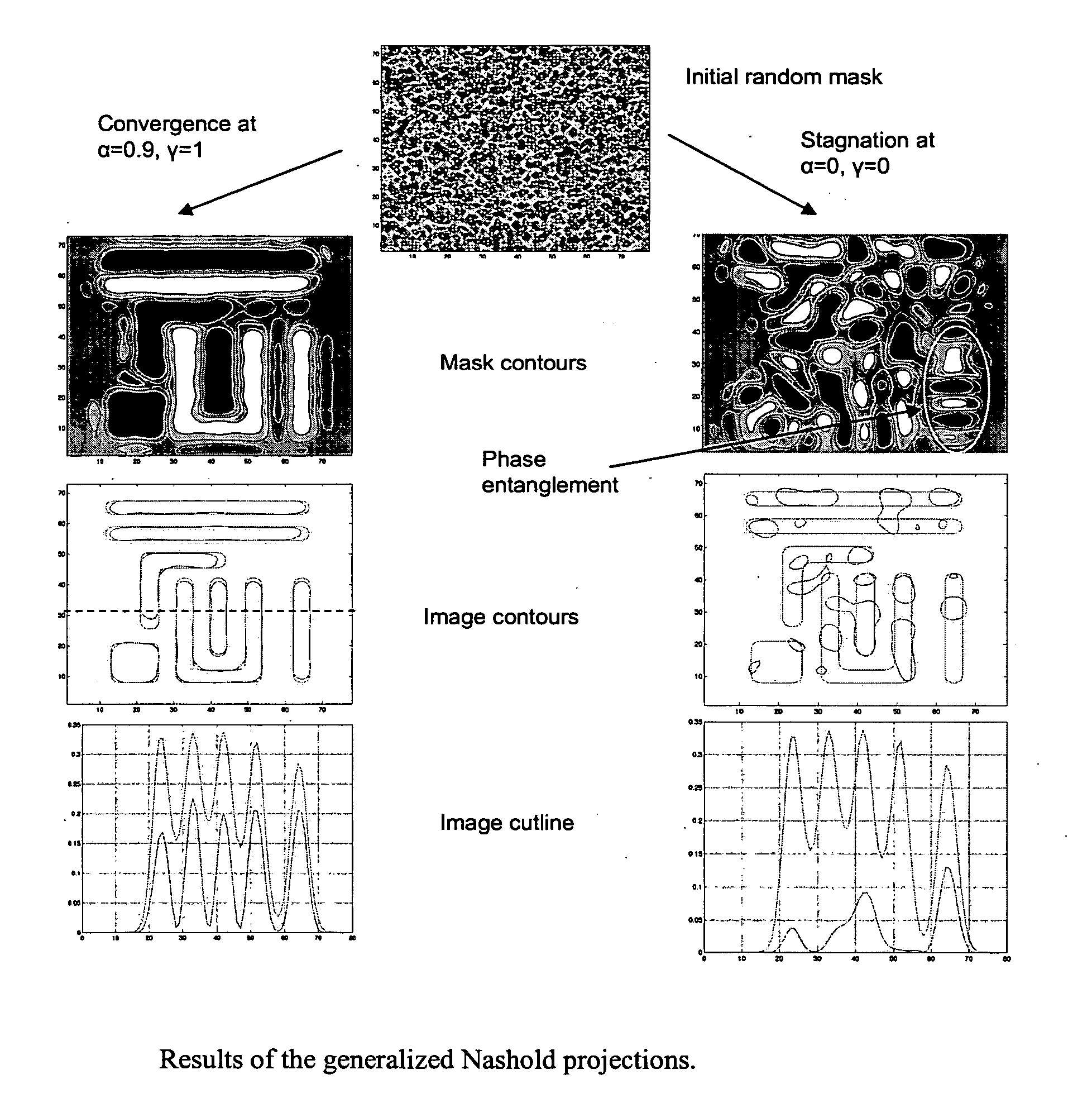
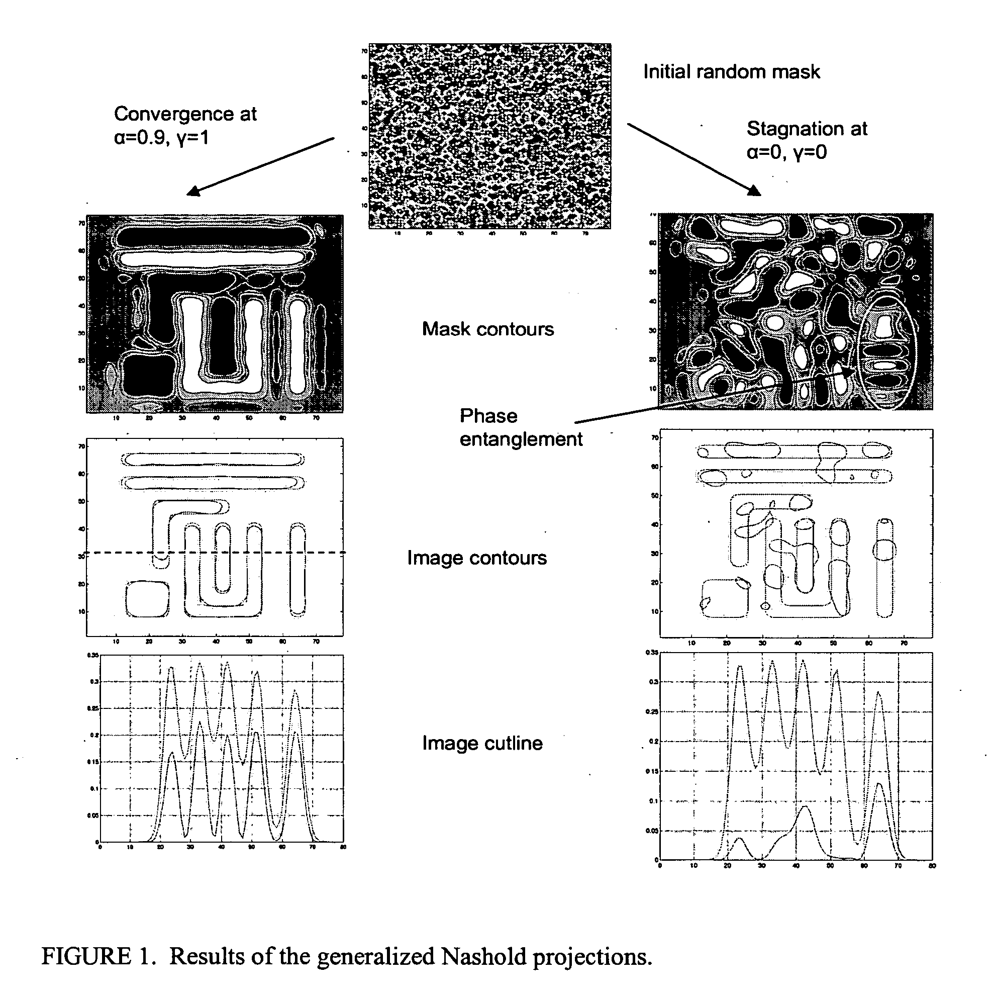
  • Figure 1
    Figure 1
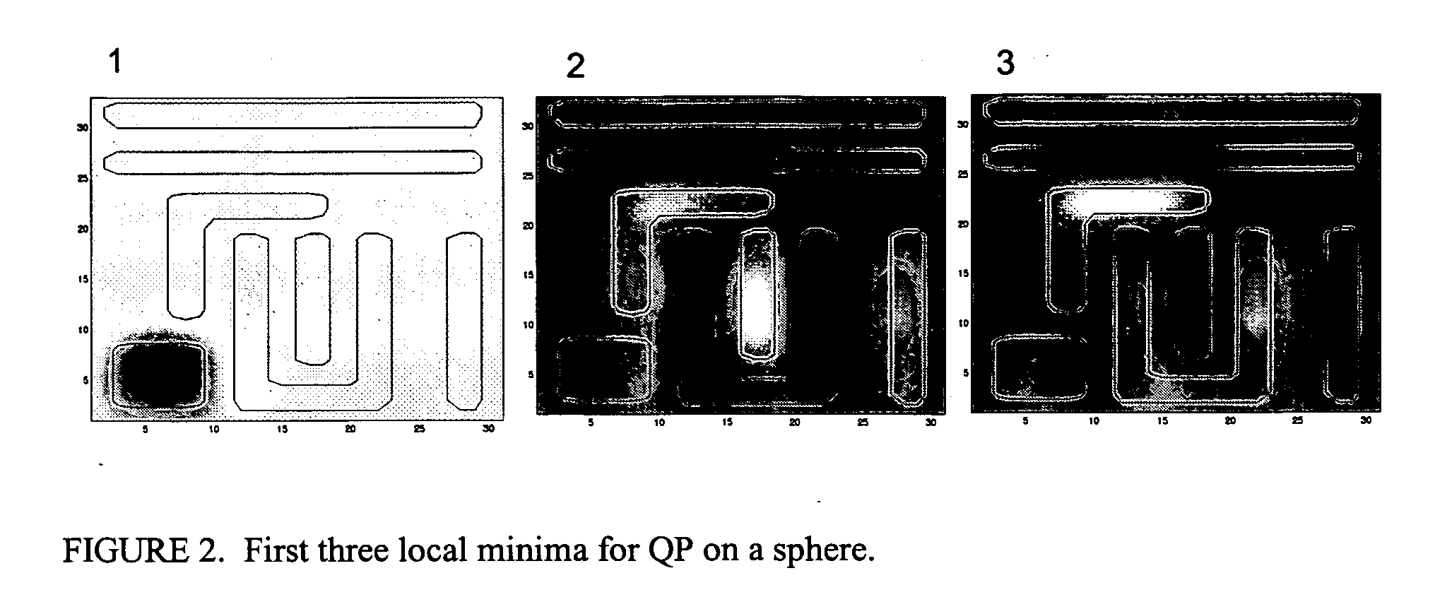
  • Figure 2
    Figure 2
  • Figure 3
    Figure 3
Patent Text Reader

Abstract

A system for calculating mask data to create a desired layout pattern on a wafer reads all or a portion of a desired layout pattern. Mask data having pixels with transmission characteristics is defined along with corresponding optimal mask data pixel transmission characteristics. An objective function is defined having one or more penalty functions that promote solutions representing a desired resolution enhancement technique. Optimization of the objective function determines the transmission characteristics of the pixels in the mask data that is used to create one or more corresponding masks or reticles.
Need to check novelty before this filing date? Find Prior Art

Description

CROSS-REFERENCE(S) TO RELATED APPLICATION(S)

[0001] The present invention claims the benefit of U.S. Provisional Patent Application Ser. No. 60 / 657,260 filed Feb. 28, 2005; U.S. Provisional Patent Application Ser. No. 60 / 658,278, filed Mar. 2, 2005; and U.S. Provisional Patent Application Ser. No. 60 / 722,840 filed Sep. 30, 2005, which are all expressly incorporated by reference herein.FIELD OF THE INVENTION

[0002] The present invention relates to photolithography, and in particular to methods of creating a semiconductor mask or reticle to print a desired layout pattern. BACKGROUND OF THE INVENTION

[0003] With conventional photolithographic processing techniques, integrated circuits are created on a semiconductor wafer by exposing photosensitive materials on the wafer through a mask or reticle. The wafer is then chemically and mechanically processed to build up the integrated circuit or other device on a layer-by-layer basis.

[0004] As the components of the integrated circuit or othe...

Examples

Embodiment Construction

[0029] As will be explained in further detail below, the present invention is a method and apparatus for calculating a mask pattern that will print a desired layout or portion thereof on a wafer. FIG. 19 illustrates a representative computer system that can be used to calculate a mask layout pattern in accordance with one embodiment of the present invention. A computer system 50, including one or more programmable processors, receives a set of executable instructions on a computer-readable media 52 such as a CD, DVD, or from a communication link such as a wired or wireless communication network such as the Internet. The computer system 50 executes the instructions to read all or a portion of a desired layout file from a database 54 or other storage media. The computer system 50 then calculates data for a mask layout by dividing a mask layout into a number of discrete pixels. The computer system determines the transmission characteristic of each of the pixels so that the result on a ...