Semiconductor device having plural bird's beaks of different sizes and manufacturing method thereof

a technology of semiconductor memory and bird's beak, which is applied in the direction of semiconductor memory devices, basic electric elements, electrical apparatus, etc., can solve the problems of deterioration of transistor characteristics, incompatibility between the bird's beak required in the memory cell transistor and the large bird's beak required in the peripheral circuit, and the concentration of electrical field in the gate edge of the transistor for the peripheral circuit cannot be avoided

Inactive Publication Date: 2006-11-30
RENESAS TECH CORP
View PDF1 Cites 14 Cited by
  • Summary
  • Abstract
  • Description
  • Claims
  • Application Information

AI Technical Summary

Benefits of technology

[0008] An object of the present invention is to provide a semiconductor device where bird's beaks in thermal oxide films are made to be different from each other between memory cell transistors and transistors for a peripheral circuit, so that

Problems solved by technology

As a result, the thickness of the gate insulating film becomes effectively large.
Therefore, small bird's beaks that are required in the memory cell transistors and large bird's beaks that are required in the transistors for the peripheral circuits are not com

Method used


Image

  • Semiconductor device having plural bird's beaks of different sizes and manufacturing method thereof
  • Semiconductor device having plural bird's beaks of different sizes and manufacturing method thereof
  • Semiconductor device having plural bird's beaks of different sizes and manufacturing method thereof

Examples


first embodiment

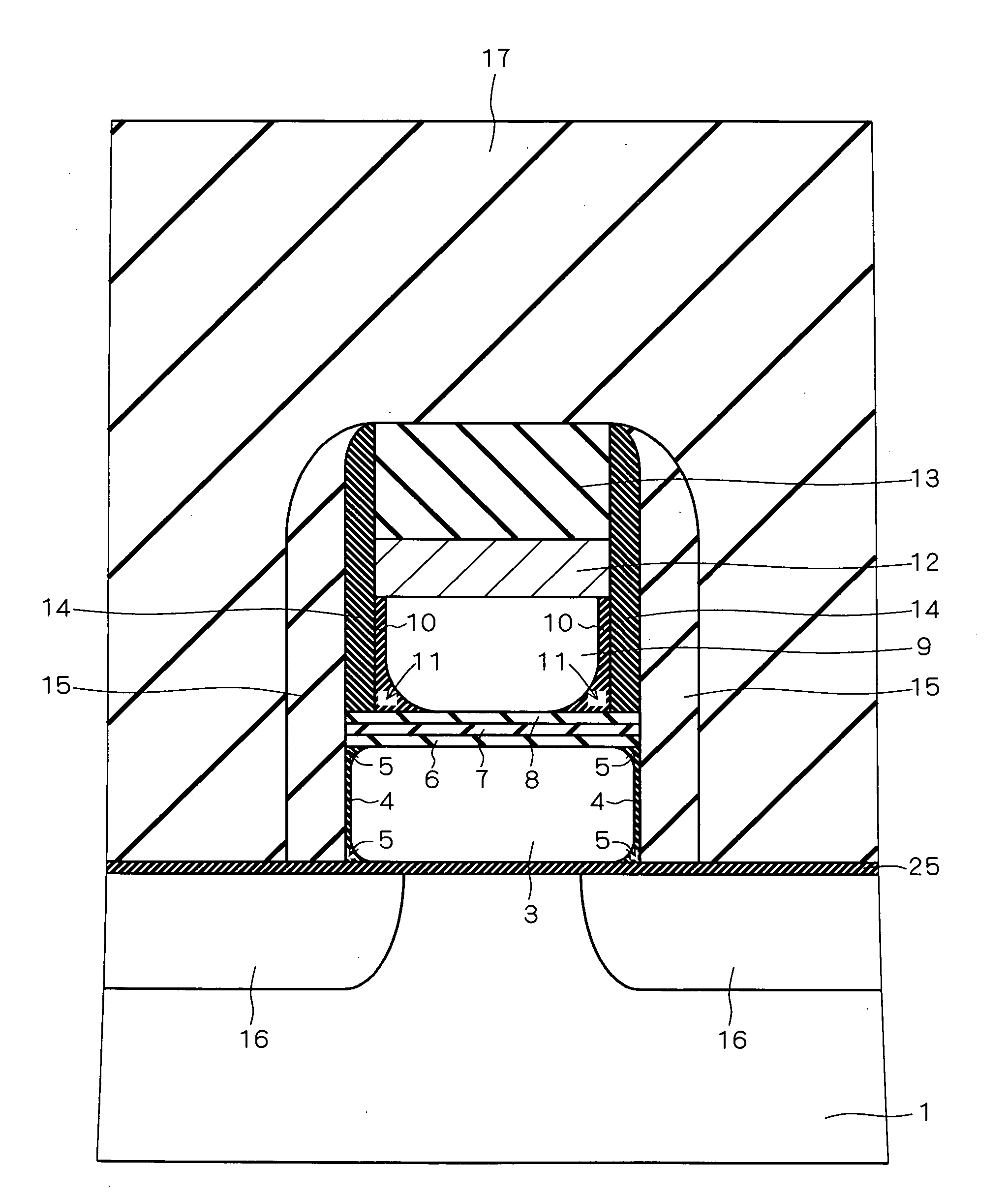
[0029]FIG. 1 is a cross-sectional view showing the structure of a memory cell transistor according to a first embodiment of the present invention, and FIG. 12 is a cross-sectional view showing the structure of a transistor for a peripheral circuit according to the first embodiment. The memory cell transistor shown in FIG. 1 is formed in a memory cell array region of a silicon substrate 1, and the transistor for the peripheral circuit shown in FIG. 12 is formed in a peripheral circuit region of the same silicon substrate 1.

[0030] With reference to FIG. 1, a tunnel oxide film 2 is formed on the upper surface of the silicon substrate 1. A floating gate 3 is formed on the upper surface of the tunnel oxide film 2. Thermal oxide films 4 are formed in the side surfaces of the floating gate 3. A silicon oxide film 6, a silicon nitride film 7 and a silicon oxide film 8 are formed in this order on the upper surface of the floating gate 3. An insulating film having a three-layer structure whe...

second embodiment

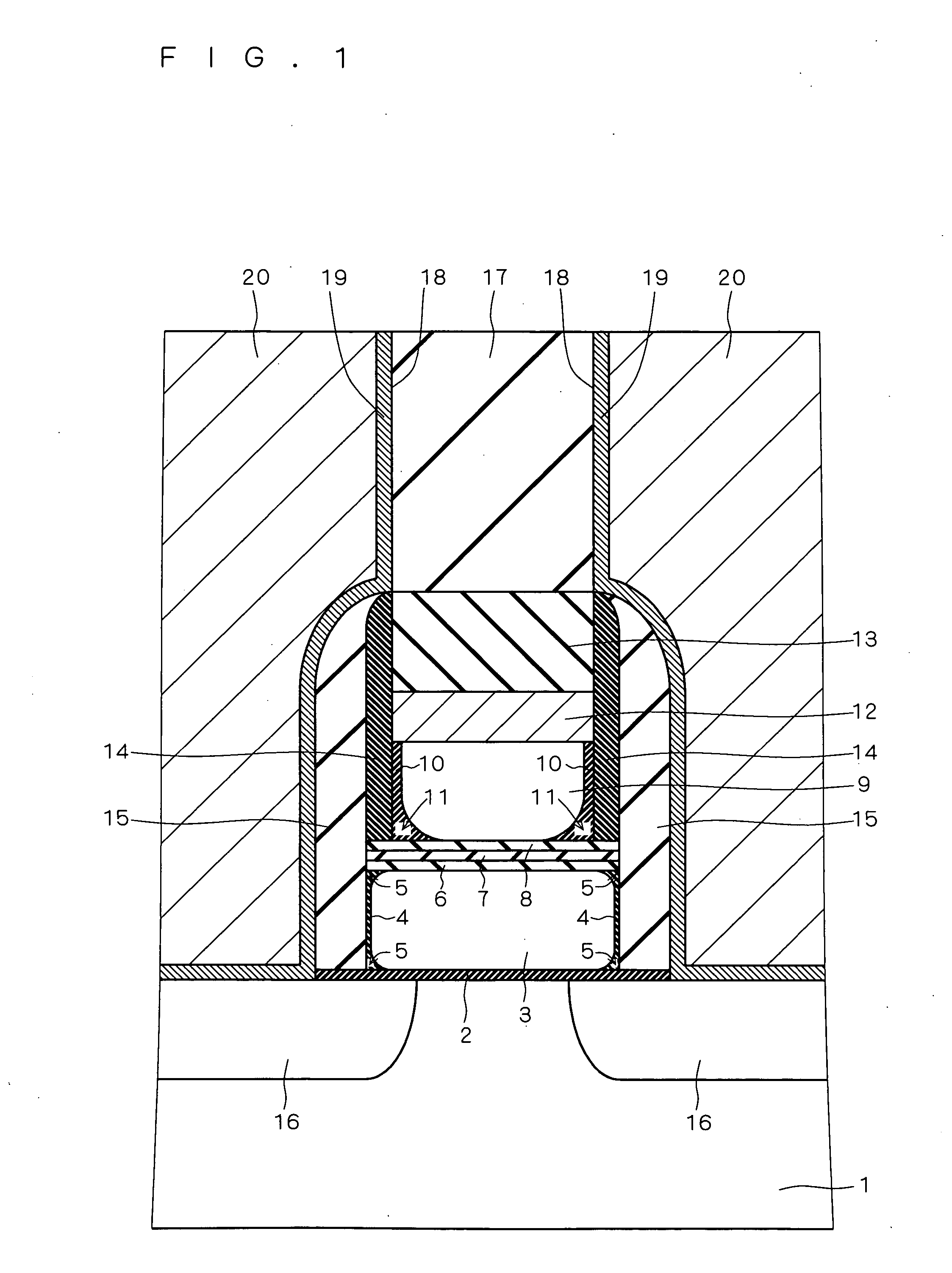
[0056]FIG. 22 is a cross-sectional view showing the structure of a memory cell transistor according to a second embodiment of the present invention, and FIG. 30 is a cross-sectional view showing the structure of a transistor for a peripheral circuit according to the second embodiment. The memory cell transistor shown in FIG. 22 is formed in a memory cell array region of a silicon substrate 1, and the transistor for the peripheral circuit shown in FIG. 30 is formed in the peripheral circuit region of the same silicon substrate 1.

[0057] With reference to FIG. 22, a tunnel oxide film 2 is formed on the upper surface of the silicon substrate 1. A floating gate 3 is formed on the upper surface of the tunnel oxide film 2. Thermal oxide films 4 are formed in the side surfaces of the floating gate 3. An ONO film where a silicon oxide film 6, a silicon nitride film 7 and a silicon oxide film 8 are layered in this order is formed on the upper surface the floating gate 3.

[0058] A control gat...

third embodiment

[0082] In the first and second embodiments, description has been given that the size of bird's beaks in a memory cell transistor is different from the size of bird's beaks in a transistor for a peripheral circuit. Transistors for peripheral circuits, however, can be divided into transistors for low-voltage system peripheral circuits that are driven by a relatively low voltage, and transistors for high-voltage system peripheral circuits that are driven by a relatively high voltage.

[0083] As for the transistor for a low-voltage system peripheral circuit, in the case where the gate length becomes 0.20 μm or less as a result of miniaturization of the semiconductor device, transistor characteristics deteriorate, in the same manner as in a memory cell transistor. Meanwhile, as for the transistor for a high-voltage system peripheral circuit, a high voltage (5 to 40 V) is applied to the gate electrode; therefore, it is necessary to make the bird's beaks large so as to suppress the concentr...


PUM


Abstract

First bird's beaks are respectively formed in first thermal oxide films at the bottom surface ends and the upper surface ends of a floating gate. In addition, second bird's beaks are formed in second thermal oxide films at the bottom surface ends of a control gate. The dimension of the first thermal oxide films in a gate length direction is smaller than the dimension of the second thermal oxide films in the gate length direction. The first bird's beaks are smaller than the second bird's beaks. In addition, the first bird's beaks are smaller than third bird's beaks (FIG. 12) which are formed in third thermal oxide films at the bottom surface ends of the gate electrode (polysilicon film) of a transistor for a peripheral circuit.

Description

BACKGROUND OF THE INVENTION [0001] 1. Field of the Invention [0002] The present invention relates to a semiconductor device and a manufacturing method thereof. In particular, the present invention relates to a nonvolatile semiconductor memory device where memory cell transistors and transistors for a peripheral circuit are formed using the same semiconductor substrate, and a manufacturing method thereof. [0003] 2. Description of the Background Art [0004] According to a conventional manufacturing method of a nonvolatile semiconductor memory device where memory cell transistors and transistors for a peripheral circuit are formed using the same semiconductor substrate, the respective side surfaces of floating gates and control gates of the memory cell transistors and the side surfaces of the gate electrodes of the transistors for the peripheral circuit are thermally oxidized in the same process for the purpose of alleviation of the electrical field at the gate ends and recovery of the ...

Claims


Application Information

Patent Timeline
IPC IPC(8): H01L29/94H01L21/76
CPCH01L21/28273H01L21/823437H01L21/823462H01L21/823468H01L29/7881H01L27/11526H01L27/11546H01L29/42324H01L29/66825H01L27/105H01L29/40114H10B41/49H10B41/40
Inventor TSUNOMURA, TAKAAKISUMINO, JUN
Owner RENESAS TECH CORP
Why Eureka
Try Eureka