

Semiconductor device
- Summary
- Abstract
- Description
- Claims
- Application Information
AI Technical Summary
Benefits of technology
Problems solved by technology
Method used
Image

Examples
first embodiment
[0051] A first embodiment of the invention is a semiconductor device including a semiconductor layer in which plural band gap change thin films are continuously laminated, a band gap being continuously monotonously changed in a laminating direction in the band gap change thin film, wherein directions in which the band gaps of at least the two adjacent band gap change thin films are monotonously changed are equal to each other in the semiconductor layer.
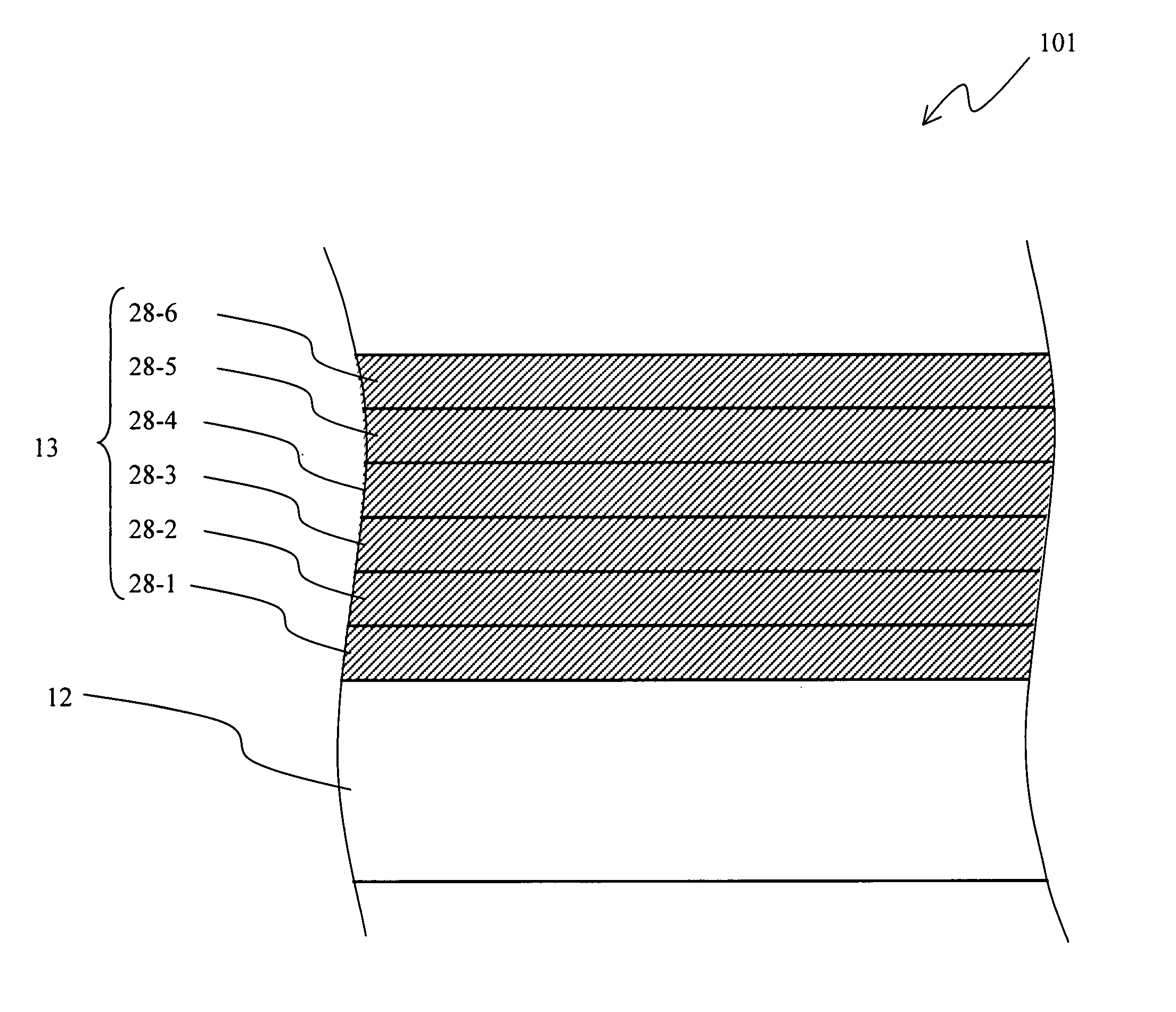
[0052]FIG. 1 is a sectional view schematically showing a semiconductor device 101 according to the first embodiment of the invention. The semiconductor device 101 sequentially includes a substrate 12 and a first semiconductor layer 13. The first semiconductor layer 13 includes plural band gap change thin films 28 in the laminating direction.
[0053] Referring to FIG. 1, branched numbers are sequentially added to the band gap change thin films 28 from the side of the substrate 12. In the following description, when the band gap change ...
second embodiment
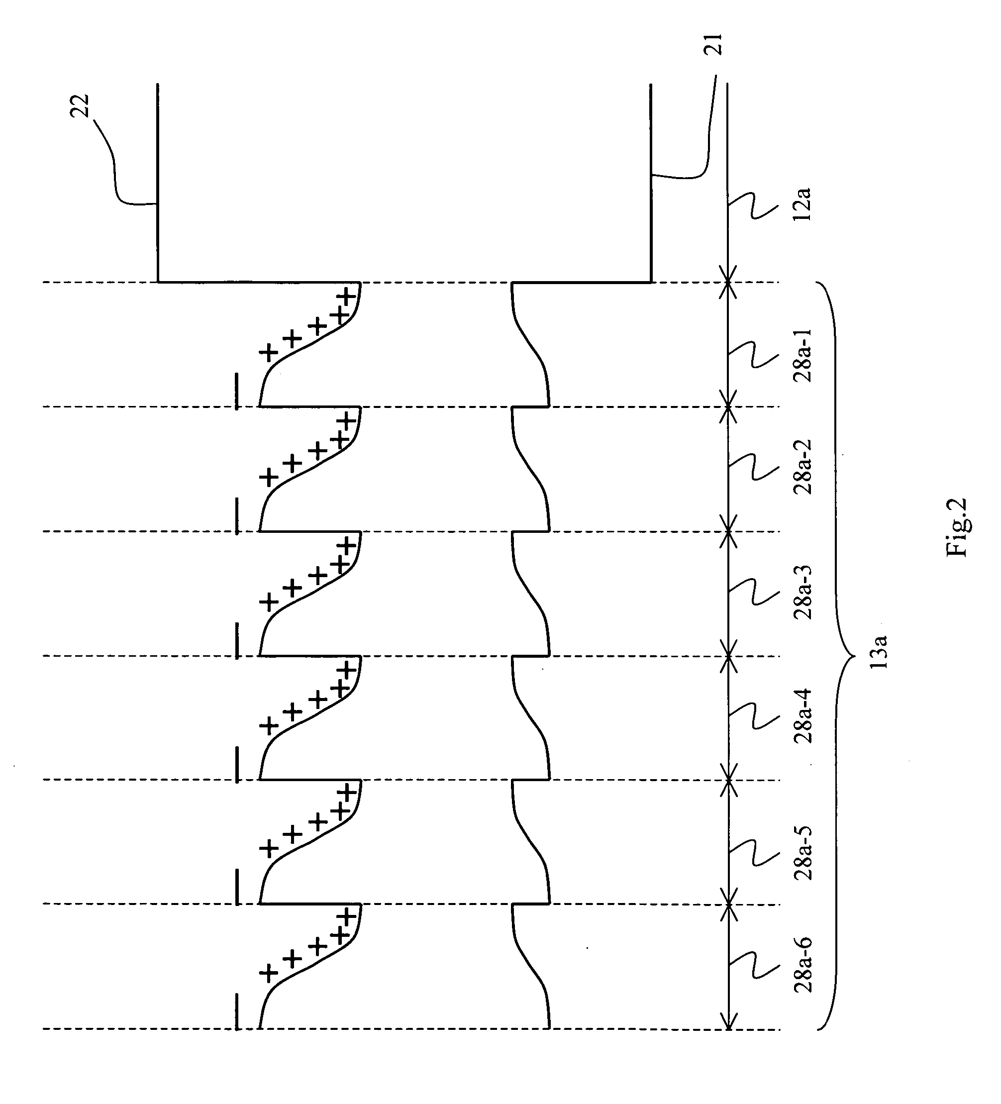
[0075]FIG. 3 is a sectional view schematically showing a semiconductor device 103 according to a second embodiment of the invention. The semiconductor device 103 sequentially includes the substrate 12 and a second semiconductor layer 33. In FIG. 3, the same layer or thin film as FIG. 1 is designated by the same numeral, and the same layer or thin film has the same function. The semiconductor device 103 differs from the semiconductor device 101 in that the semiconductor device 103 does not include the first semiconductor layer 13, but the semiconductor device 103 includes the second semiconductor layer 33. The second semiconductor layer 33 includes the plural band gap change thin films 48 in the laminating direction. When the band gap change thin film 48 without adding the branched number, the description is given in common with all the band gap change thin films 48.
[0076] Similarly to the band gap change thin film 28, the band gap change thin film 48 is a semiconductor thin film in...
third embodiment
[0086] A third embodiment of the invention is a semiconductor device including a semiconductor layer in which plural band gap change thin films are continuously laminated, a band gap being continuously monotonously changed in a laminating direction in the band gap change thin film, wherein directions in which the band gaps of at least the two adjacent band gap change thin films are monotonously changed are opposite to each other in the semiconductor layer.
[0087]FIG. 5 is a sectional view schematically showing a semiconductor device 105 according to the third embodiment of the invention. The semiconductor device 105 sequentially includes the substrate 12 and a third semiconductor layer 53. In FIG. 5, the same layer or thin film as FIG. 1 is designated by the same numeral, and the same layer or thin film has the same function. The semiconductor device 105 differs from the semiconductor device 101 of FIG. 1 in that the semiconductor device 105 does not include the first semiconductor ...
PUM
 Abstract
Description
Claims
Application Information