Cluster tool architecture for processing a substrate

a technology of clustering tools and substrates, applied in the field of integrated processing systems, can solve the problems of limiting the throughput of the processing sequence, wasting a large amount of time for clustering tool users and manufacturers, and consuming a large amount of tim

Active Publication Date: 2006-12-14
APPLIED MATERIALS INC
View PDF99 Cites 12 Cited by
  • Summary
  • Abstract
  • Description
  • Claims
  • Application Information

AI Technical Summary

Benefits of technology

[0014] Embodiments of the invention further provide a cluster tool for processing a substrate, comprising a first processing rack containing a first vertical stack of substrate processing chambers, a first robot adapted to transfer a substrate to a substrate processing chamber in the first processing rack, a second processing rack containing a first vertical stack of substrate processing chambers, a second robot adapted to transfer a substrate between a substrate processing chamber in the first processing rack and a substrate processing chamber in the second processing rack, a controller that is adapted to optimize the movements of the substrate through the first and second processing rack using the first robot or second robot, and a memory, coupled to the controller, the memory comprising a computer-readable medium having a computer-readable program embodied therein for directing the operation of the cluster tool, the computer-readable program comprising computer instructions to control the first robot and second robot movement comprising storing one or more command tasks for the first robot and second robot in the memory, review command tasks for first robot retained in the memory, review command tasks for second robot retained in the memory, and move command tasks from the first robot to the second robot or the second robot to the first robot to balance the availability of each robot.

Problems solved by technology

In an effort to reduce CoO, electronic device manufacturers often spend a large amount of time trying to optimize the process sequence and chamber processing time to achieve the greatest substrate throughput possible given the cluster tool architecture limitations and the chamber processing times. In track lithography type cluster tools, since the chamber processing times tend to be rather short, (e.g., about a minute to complete the process) and the number of processing steps required to complete a typical process sequence is large, a significant portion of the time it takes to complete the processing sequence is taken up transferring the substrates between the various processing chambers.
If the substrate throughput in a cluster tool is not robot limited, the longest process recipe step will generally limit the throughput of the processing sequence.
This is usually not the case in track lithography process sequences, due to the short processing times and large number of processing steps.
These factors are very important to a cluster tool's profitability and / or usefulness, since the longer the system is unable to process substrates the more money is lost by the user due to the lost opportunity to process substrates in the cluster tool.
Therefore, cluster tool users and manufacturers spend a large amount of time trying to develop reliable processes, reliable hardware and reliable systems that have increased uptime.
The push in the industry to shrink the size of semiconductor devices to improve device processing speed and reduce the generation of heat by the device, has caused the industry's tolerance to process variability to diminish.
Due to the shrinking size of semiconductor devices and the ever increasing device performance requirements, the allowable variability of the device fabrication process uniformity and repeatability has greatly decreased.
Lithography type device fabrication processes can be especially sensitive to variations in process recipe variables and the timing between the recipe steps, which directly affects process variability and ultimately device performance.

Method used


Image

  • Cluster tool architecture for processing a substrate
  • Cluster tool architecture for processing a substrate
  • Cluster tool architecture for processing a substrate

Examples


Embodiment Construction

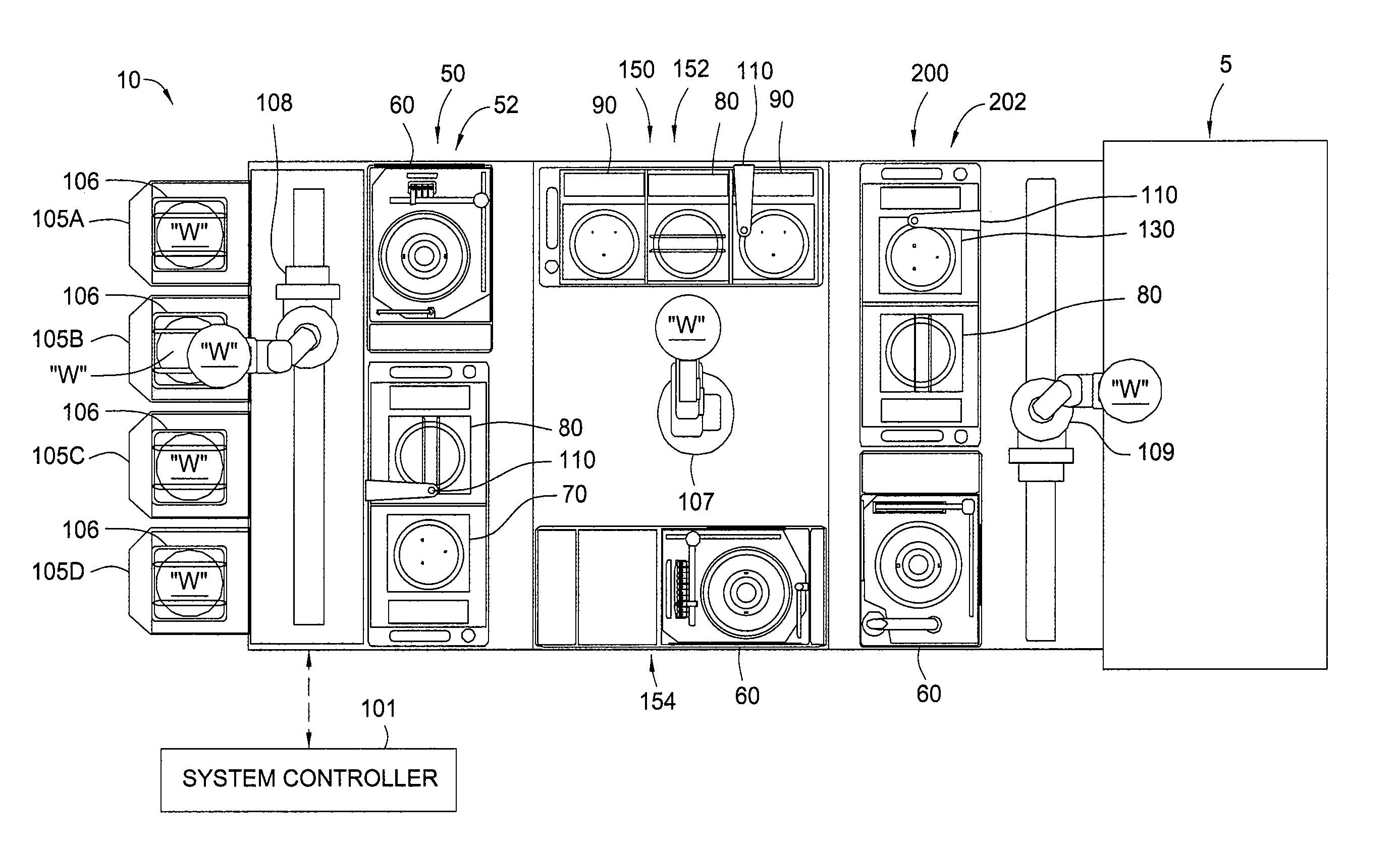
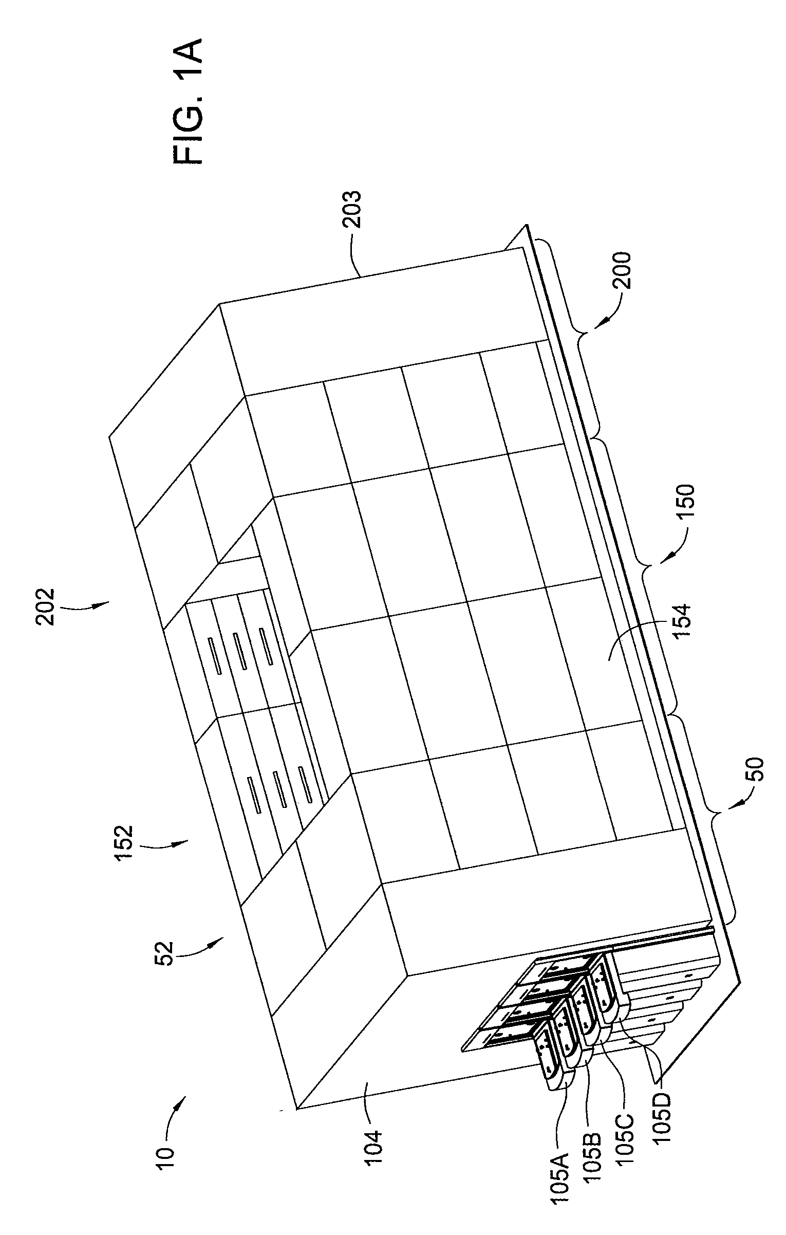
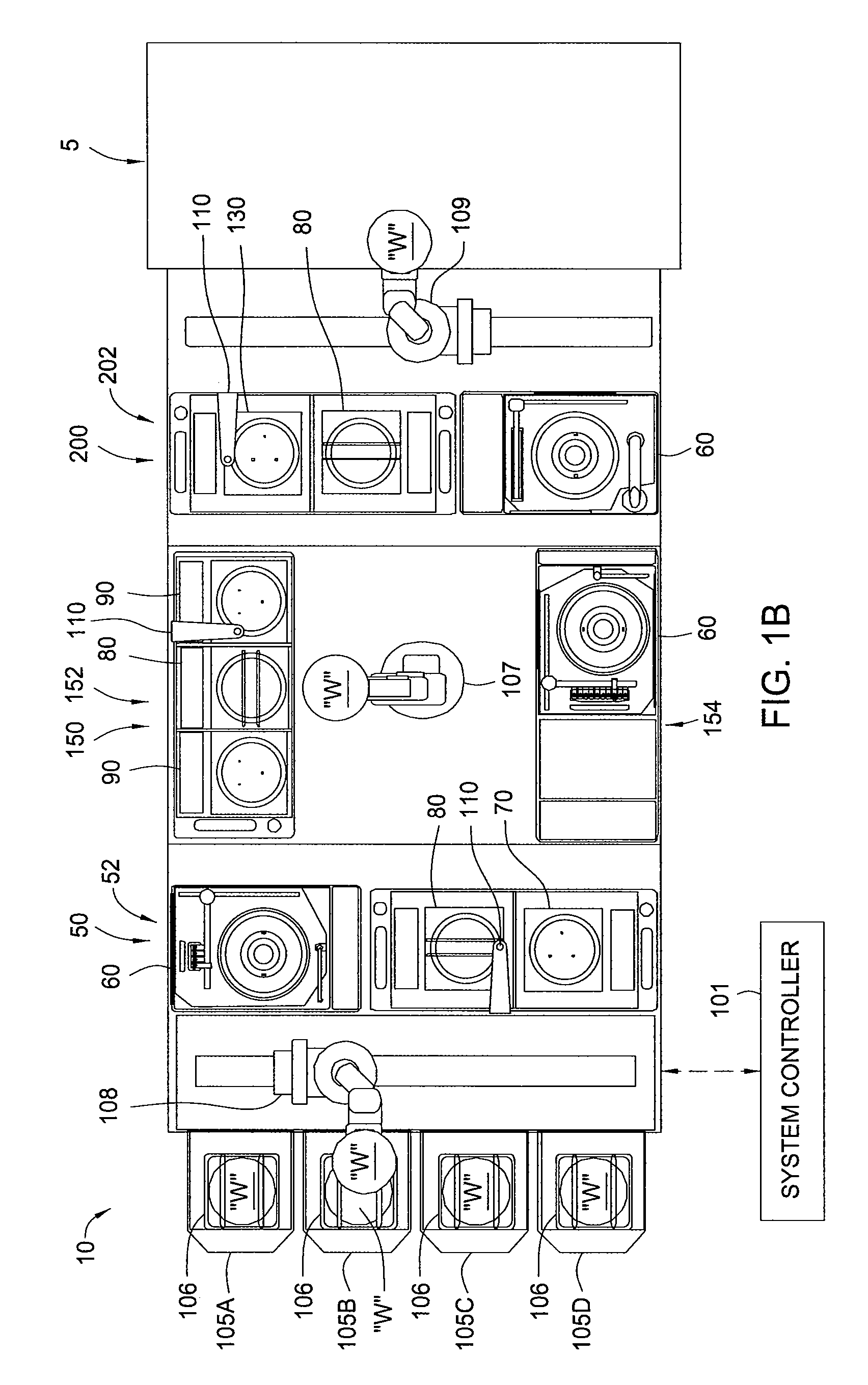
[0108] The present invention generally provides an apparatus and method for processing substrates using a multi-chamber processing system (e.g., a cluster tool) that has an increased system throughput, increased system reliability, more repeatable wafer processing history (or wafer history) within the cluster tool, and also a reduced footprint of the cluster tool. In one embodiment, the cluster tool is adapted to perform a track lithography process in which a substrate is coated with a photosensitive material, is then transferred to a stepper / scanner, which exposes the photosensitive material to some form of radiation to form a pattern in the photosensitive material, and then certain portions of the photosensitive material are removed in a developing process completed in the cluster tool.

[0109]FIGS. 1A and 1C are isometric views of one embodiment of a cluster tool 10 that illustrates a number of the aspects of the present invention that may be used to advantage. One embodiment of t...


PUM

PropertyMeasurementUnit
distanceaaaaaaaaaa
distanceaaaaaaaaaa
temperatureaaaaaaaaaa

Abstract

Embodiments generally provide an apparatus and method for processing substrates using a multi-chamber processing system (e.g., a cluster tool) that has an increased system throughput, increased system reliability, substrates processed in the cluster tool have a more repeatable wafer history, and also the cluster tool has a smaller system footprint. In one embodiment, the cluster tool is adapted to perform a track lithography process in which a substrate is coated with a photosensitive material, is then transferred to a stepper / scanner, which exposes the photosensitive material to some form of radiation to form a pattern in the photosensitive material, which is then removed in a developing process completed in the cluster tool. In track lithography type cluster tools, since the chamber processing times tend to be rather short, and the number of processing steps required to complete a typical track system process is large, a significant portion of the time it takes to process a substrate is taken up by the processes of transferring the substrates in a cluster tool between the various processing chambers. In one embodiment of the cluster tool, the cost of ownership is reduced by grouping substrates together and transferring and processing the substrates in groups of two or more to improve system throughput, and reduces the number of moves a robot has to make to transfer a batch of substrates between the processing chambers, thus reducing wear on the robot and increasing system reliability. In one aspect of the invention, the substrate processing sequence and cluster tool are designed so that the substrate transferring steps performed during the processing sequence are only made to chambers that will perform the next processing step in the processing sequence. Embodiments also provide for a method and apparatus that are used to improve the coater chamber, the developer chamber, the post exposure bake chamber, the chill chamber, and the bake chamber process results. Embodiments also provide for a method and apparatus that are used to increase the reliability of the substrate transfer process to reduce system down time.

Description

CROSS-REFERENCE TO RELATED APPLICATIONS [0001] This application is a continuation of U.S. patent application Ser. No. 11 / 112,281, filed Apr. 22, 2005, which claims benefit of U.S. provisional patent application Ser. No. 60 / 639,109 filed Dec. 22, 2004, which are both herein incorporated by reference.BACKGROUND OF THE INVENTION [0002] 1. Field of the Invention [0003] Embodiments of the invention generally relate to an integrated processing system containing multiple processing stations and robots that are capable of processing multiple substrates in parallel. [0004] 2. Description of the Related Art [0005] The process of forming electronic devices is commonly done in a multi-chamber processing system (e.g., a cluster tool) that has the capability to sequentially process substrates, (e.g., semiconductor wafers) in a controlled processing environment. A typical cluster tool used to deposit (i.e., coat) and develop a photoresist material, commonly known as a track lithography tool, will ...

Claims


Application Information

Patent Timeline
Patent Type & Authority Applications(United States)
IPC IPC(8): C23C16/00
CPCH01L21/67173H01L21/67745H01L22/26H01L21/67196H01L21/6831G03B27/32Y10S414/136H01L21/67109H01L21/68707H01L21/67742H01L21/6719G03F7/40Y10T29/53187H01L21/67161Y10S414/135H01L21/67754H01L21/67178G03D13/006H01L21/67748G05B2219/40476Y10T29/5323G05B19/41825H01L21/67184G05B2219/49137H01L21/6838H01L21/6715G05B2219/45031H01L21/67225Y02P90/02
Inventor ISHIKAWA, TETSUYAROBERTS, RICK J.ARMER, HELEN R.VOLFOVSKI, LEONPINSON, JAY D.RICE, MICHAELQUACH, DAVID H.SALEK, MOHSEN S.LOWRANCE, ROBERTBACKER, JOHN A.WEAVER, WILLIAM TYLERCARLSON, CHARLESWANG, CHONGYANGHUDGENS, JEFFREYHERCHEN, HARALDLUE, BRIAN
Owner APPLIED MATERIALS INC
Why Eureka
Try Eureka