Voltage conversion circuit and switching power supply device
a voltage conversion circuit and switching power supply technology, applied in the direction of electric variable regulation, process and machine control, instruments, etc., can solve the problems of large loss of electric power by the transistor qb, and the inability of auxiliary power supply circuits with high efficiency to be configured in the switching power supply device, so as to achieve low loss of input ac voltage or power supply voltage, the effect of good respons
- Summary
- Abstract
- Description
- Claims
- Application Information
AI Technical Summary
Benefits of technology
Problems solved by technology
Method used
Image
Examples
first embodiment
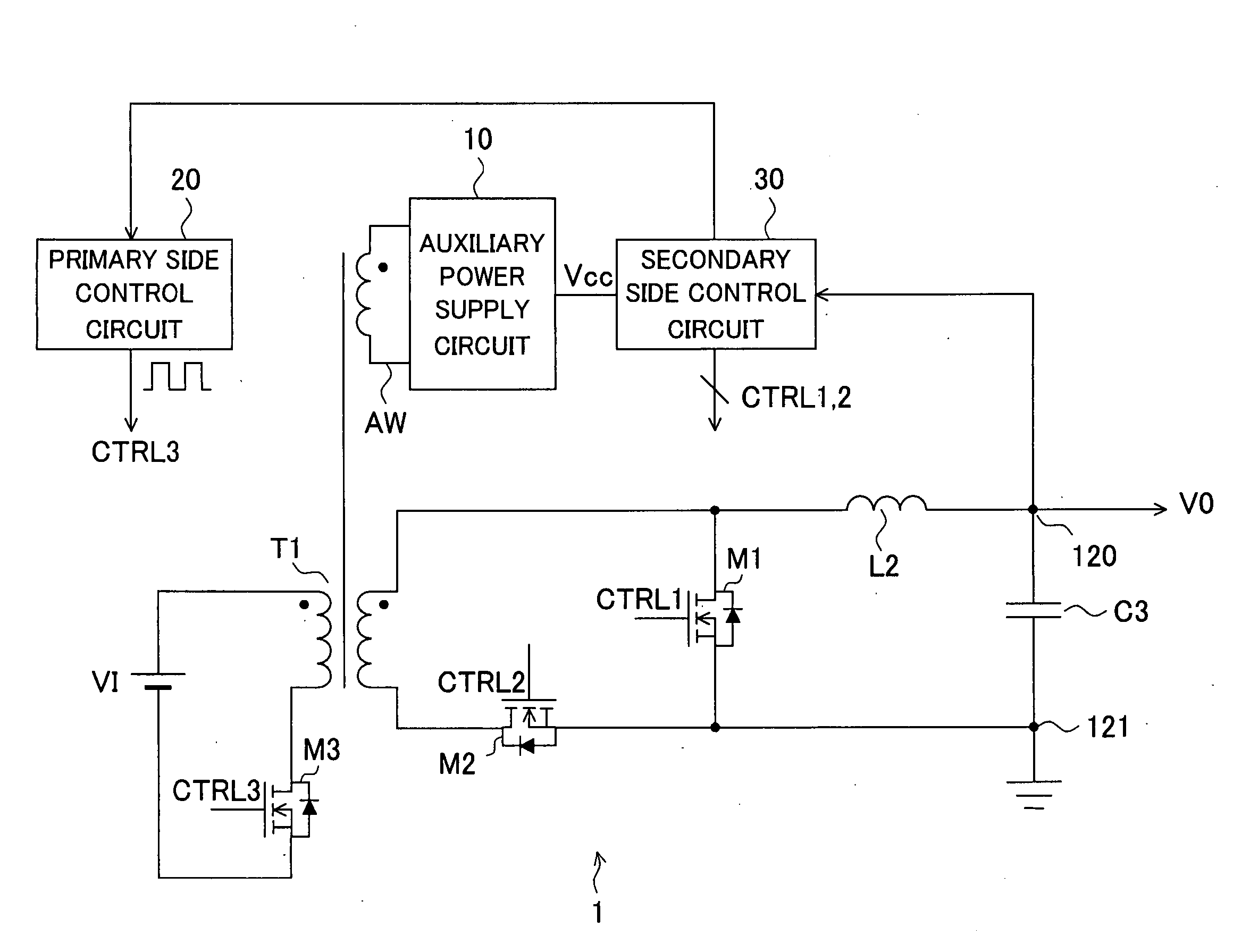
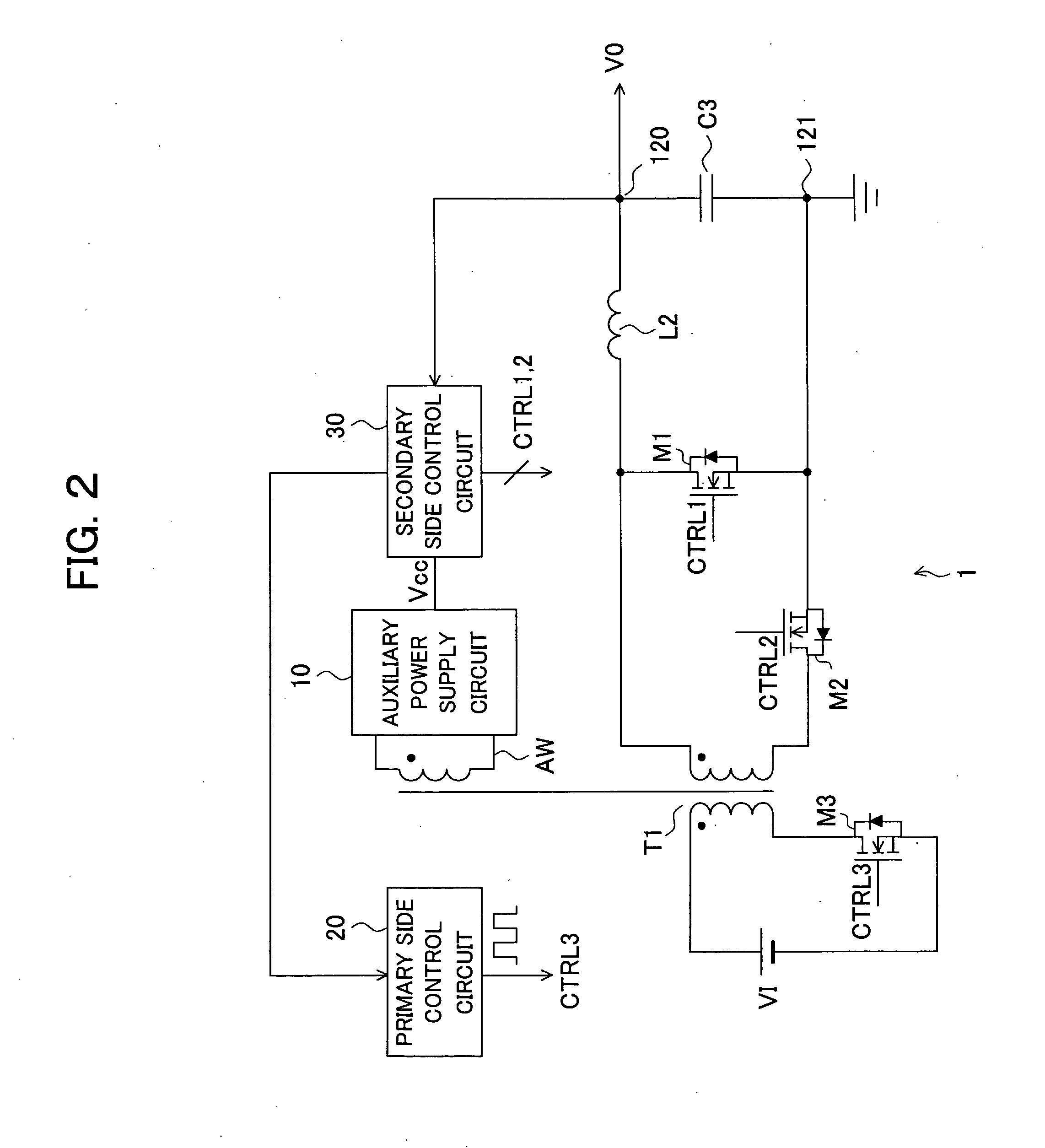
[0023] First Embodiment FIG. 2 is a diagram of the system configuration of a switching power supply device 1 according to an embodiment of the present invention. In the present embodiment, as an example, a forward type switching power supply device 1 is described below. In the forward type switching power supply device 1, an input voltage VI is given to a primary side of the transformer T1. The transformer T1 is given a pulse width modulation (PWM) signal using the input voltage VI as a peak voltage by the switch operation of an NMOS transistor M3. The PWM signal is transmitted to the secondary side with the same polarity by the transformer T1.
[0024] On the secondary side of the transformer T1, a coil L2 is connected between one end of the secondary winding and a node 120 (output terminal), and a capacitor C3 is connected between the node 120 (output terminal) and a node 121 (ground terminal) to thereby configure a smoothing circuit of choke input type. Further, the rectification ci...
second embodiment
[0044] Second Embodiment
[0045] Next, a second embodiment of the present invention is described. In the present embodiment, there is described below the mode of assembling the power supply voltage generation circuit of the present invention in a synchronized rectification circuit of a current doubler type switching power supply device. FIG. 5 is a diagram showing the circuit configuration of a synchronized rectification circuit 50 on the secondary side of the transformer T1 in a switching power supply device 2 according to the present embodiment.
[0046] In the switching power supply device 2, under the control of a not shown primary side, the transformer T1 is controlled so as to alternately output a plus voltage and a minus voltage, turn off a rectifier constituted by the NMOS transistor M10 when outputting the plus voltage, and turn off a rectifier constituted by the NMOS transistor M20 when outputting the minus voltage. Note that when there is no output from the transformer T1, bo...
PUM
 Abstract
Description
Claims
Application Information


