Scan test design method, scan test circuit, scan test circuit insertion cad program, large-scale integrated circuit and mobile digital equipment

Inactive Publication Date: 2006-12-14
PANASONIC CORP
View PDF4 Cites 26 Cited by
  • Summary
  • Abstract
  • Description
  • Claims
  • Application Information

AI Technical Summary

Benefits of technology

[0037] In addition, in the scan test circuit insertion CAD program of the present invention, which has a design algorithm of connecting a plurality of scan flipflop circuits driven with each of final-stage elements of the clock tree in series to form a scan shift register, insertion of the scan test circuit can be made automatically. Also, the design algorithm can be used at the same design stage as the conventional scan chain wiring optimization functi

Problems solved by technology

This disadvantageously increases the circuit area, the power consumption and the leak current during standby of a number of delay elements.
Moreover, in the conventional circuit in which FF circuits of different clock tree lines are connected to each other, as in the example of FIG. 2, when design adopts a semiconductor microfabrication process, which is significantly susceptible to interference such as crosstalk and IR drop, the delay time in the clock tree portion will be affected by such

Method used


Image

  • Scan test design method, scan test circuit, scan test circuit insertion cad program, large-scale integrated circuit and mobile digital equipment
  • Scan test design method, scan test circuit, scan test circuit insertion cad program, large-scale integrated circuit and mobile digital equipment
  • Scan test design method, scan test circuit, scan test circuit insertion cad program, large-scale integrated circuit and mobile digital equipment

Examples


first embodiment

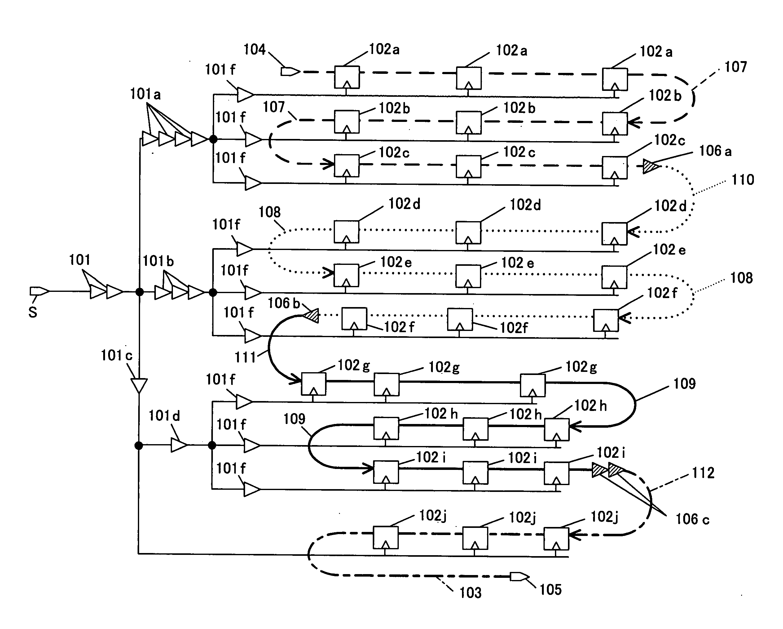
[0053]FIG. 1 shows a configuration of a scan shift register of a scan shift circuit implemented by a design-for-testability method of the first embodiment of the present invention, illustrating in particular the configuration of CTS buffers and the connection relationship in the scan shift register. This embodiment will be described with reference to FIG. 1.

[0054] Referring to FIG. 1, the reference numeral 101 denotes clock delay adjusting buffers and 101a to 101f denote CTS buffers. A clock tree T includes branching from a predetermined clock origin point or clock supply point S to the buffers 101a, 101b and 101c via the buffers 101, and each branch is further branched to three buffers 101f. A clock signal is supplied to clock terminals of a plurality of flipflop (FF) circuits 102a to 102j via the clock tree T.

[0055] In the design method of this embodiment, first, a scan shift register is formed from a plurality of FF circuits driven with each of the final-stage elements 101f of ...

second embodiment

[0058] The second embodiment of the present invention will be described.

[0059] In FIG. 1 showing the first embodiment described above, a sub-scan chain was formed from the three FF circuits 102a. A scan shift register was also formed using the three FF circuits for each of the FF circuits 102b, 102c, 102d, 102e, 102f, 102g, 102h, 102i and 102j, as in the case of the three FF circuits 102a. In the first embodiment, therefore, a scan test circuit can be formed by connecting the inputs / outputs of the shift registers to scan inputs / outputs of the LSI. This configuration however requires a huge amount of test terminals in a large-scale circuit, causing increase in test cost and shortage of terminals due to limitations on the external terminals of the LSI. As a result, it may be difficult to implement the design for testability.

[0060] To solve the above problem, in this embodiment, the sub-scan chains described in the first embodiment are connected to each other to form a larger scan sh...

third embodiment

[0063] The third embodiment of the present invention will be described.

[0064] The third embodiment is directed to a design method to be adopted when the number of scan test terminals (scan-in terminals and scan-out terminals) yet fails to fall within the limitation on the number of terminals even in the second embodiment described above.

[0065] When the limitation on the number of scan test terminals is not yet cleared in the second embodiment or when further reduction in the number of scan chains is desired for other reasons, it becomes necessary to connect scan shift registers different in the number of stages of CTS buffers to each other. In this case, as in the second embodiment, the first priority is given to connection of shift registers equal in the number of stages of CTS buffers in series via the inter-sub-scan chain connection net 107, 108 or 109.

[0066] Subsequently, the second priority is given to connection between shift registers smallest in the relative difference in...


PUM


Abstract

In scan test circuit design, a plurality of flipflop circuits (102a, 102b or 102c) driven with each of final-stage elements 101f of a clock tree T are connected in series, to form a sub-scan chain. Also, sub-scan chains smallest in the relative difference in the number of stages of delay elements existing from the clock supply point S of the clock tree T (i.e., sub-scan chains different by one stage) are connected to each other. Further, sub-scan chains are connected so that data shift be made from a flipflop circuit larger in clock delay to a flipflop circuit smaller in clock delay. This reduces the number of delay elements inserted in data lines of a shift register for hold time guarantee in shift operation of the scan shift register, and suppresses power consumption.

Description

TECHNICAL FIELD [0001] The present invention relates to an LSI design method, an LSI test circuit and an LSI design CAD program. More particularly, the present invention relates to a design-for-testability technology that secures design guarantee on the hold time in the operation of a shift register that may cause a problem at the time of design of a scan test circuit and suppresses increase in circuit area, power consumption and leak current that may occur with insertion of hold guarantee delay elements. BACKGROUND ART [0002] Conventionally, design for testability involves scan test design most commonly. The scan test design will be described with reference to FIG. 5. [0003] Referring to FIG. 5, after RTL design, a logic synthesis CAD program 502 is executed for an RTL file 501 as input data to generate a gate-level netlist 503. Flipflop (FF) circuits constituting part of the resultant gate-level circuit 503 are first replaced with scan FF circuits under a scan test circuit inserti...

Claims


Application Information

Patent Timeline
IPC IPC(8): G01R31/28G01R31/317G01R31/3185G06F11/22G06F17/50H01L21/822H01L27/04
CPCG01R31/318575G01R31/318594G01R31/318591
Inventor HOSHAKU, MASAHIRO
Owner PANASONIC CORP
Why Eureka
Try Eureka