Grown photonic crystals in semiconductor light emitting devices

a technology of semiconductor light emitting device and photonic crystal, which is applied in the direction of crystal growth process, semiconductor laser, instruments, etc., can solve the problems of poor extraction efficiency, less than 30%, and limited extraction efficiency, so as to reduce efficiency and avoid damage

Active Publication Date: 2006-12-21
LUMILEDS
View PDF35 Cites 76 Cited by
  • Summary
  • Abstract
  • Description
  • Claims
  • Application Information

AI Technical Summary

Benefits of technology

[0010] In accordance with embodiments of the invention, a photonic crystal is grown within a semiconductor structure, such as a III-nitride structure, which includes a light emitting region disposed between an n-type region and a p-type region. The photonic crystal may be multiple regions of semiconductor material separated by a material having a different refractive index than the semiconductor material

Problems solved by technology

The extraction efficiency is limited, for example, by the emitted photons suffering multiple total internal reflections at the walls of the high refractive index semiconductor crystal that forms the p-type, n-type, and light emitting regions of the device.
As a result, many of the emitted photons do not escape into free space, leading to poor extraction efficiencies, typically less than 30%.
Howe

Method used


Image

  • Grown photonic crystals in semiconductor light emitting devices
  • Grown photonic crystals in semiconductor light emitting devices
  • Grown photonic crystals in semiconductor light emitting devices

Examples


Embodiment Construction

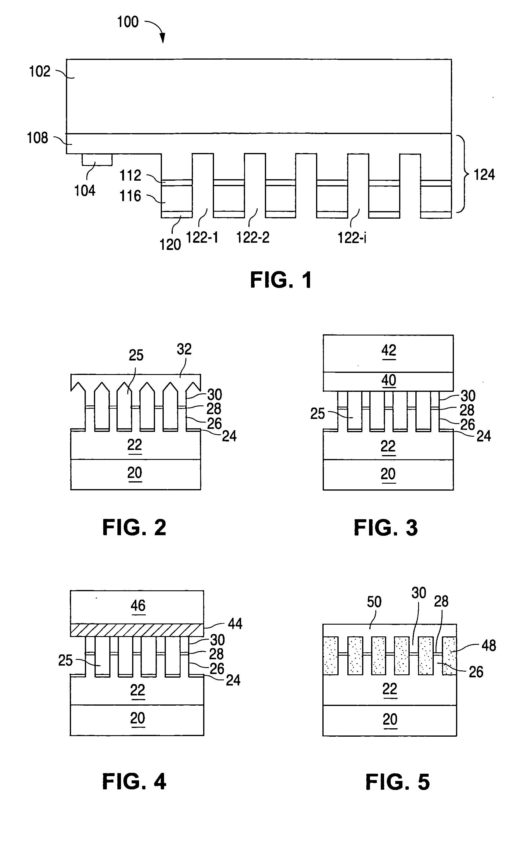
[0024]FIG. 1 illustrates a III-nitride photonic crystal LED (PXLED) 100, described in more detail in Publication No. 2003 / 0141507, “LED Efficiency Using Photonic Crystal Structure,” filed Jan. 28, 2002 and incorporated herein by reference.

[0025] In PXLED 100 of FIG. 1, an n-type region 108 is formed over growth substrate 102 which may be, for example, sapphire, SiC, or GaN; an active region 112 is formed over n-type region 108; and a p-type region 116 is formed over active region 112. Each of regions 108, 112, and 116 may be a single layer or multiple layers of the same or different composition, thickness, or dopant concentration. A portion of p-type region 116 and active region 112 are etched away to expose a portion of n-type region 108, then a p-contact 120 is formed on p-type region 116 and an n-contact 104 is formed on the exposed portion of n-type region 108. The device may be flipped over, as illustrated in FIG. 1, and connected to a mount (not shown) through contacts 104 an...


PUM


Abstract

A photonic crystal is grown within a semiconductor structure, such as a III-nitride structure, which includes a light emitting region disposed between an n-type region and a p-type region. The photonic crystal may be multiple regions of semiconductor material separated by a material having a different refractive index than the semiconductor material. For example, the photonic crystal may be posts of semiconductor material grown in the structure and separated by air gaps or regions of masking material. Growing the photonic crystal, rather than etching a photonic crystal into an already-grown semiconductor layer, avoids damage caused by etching which may reduce efficiency, and provides uninterrupted, planar surfaces on which to form electric contacts.

Description

BACKGROUND [0001] 1. Field of Invention [0002] This invention relates to semiconductor light emitting devices including photonic crystal structures. [0003] 2. Description of Related Art [0004] Light emitting devices such as light emitting diodes (“LEDs”) are technologically and economically advantageous solid state light sources. LEDs are capable of reliably providing light with high brightness, hence in the past decades they have come to play a critical role in numerous applications, including flat-panel displays, traffic lights, and optical communications. An LED includes a forward biased p-n junction. When driven by a current, electrons and holes are injected into the junction region, where they recombine and release their energy by emitting photons. Materials systems currently of interest in the manufacture of high-brightness light emitting devices capable of operation across the visible spectrum include Group III-V semiconductors, particularly binary, ternary, and quaternary al...

Claims


Application Information

Patent Timeline
IPC IPC(8): H01L27/15H01L33/08H01L33/24
CPCB82Y20/00C30B29/60G02B6/1225H01S5/34333H01L33/24H01L2933/0083H01S5/105H01L33/08H01L33/18H01S5/11H01L21/20
Inventor WIERER, JONATHAN J. JR.KRAMES, MICHAEL R.GARDNER, NATHAN F.
Owner LUMILEDS
Why Eureka
Try Eureka