Compensation currents in non-volatile memory read operations

a non-volatile memory and read operation technology, applied in the field of non-volatile memory, can solve the problems of memory cells, reducing the separation between adjacent states, and erroneous reading of data stored, and achieve the effect of increasing the apparent conduction curren

Active Publication Date: 2006-12-21
SANDISK TECH LLC
View PDF20 Cites 49 Cited by
  • Summary
  • Abstract
  • Description
  • Claims
  • Application Information

AI Technical Summary

Benefits of technology

[0015] The read process for a selected memory cell takes into account the state of one or more adjacent memory cells. If an adjacent memory cell is in one or more of a predetermined set of programmed states, a compensation current can be provided to increase the apparent conduction current of the selected memory cell. An initializati

Problems solved by technology

The coupling from adjacent memory cells can shift the apparent charge level being read from a selected memory cell by a sufficient amount to lead to an erroneous reading of the data stored.
Therefore, floating gate to floating gate coupling can result in memory cells being shifted from an allowed threshold voltage range to a fo

Method used


Image

  • Compensation currents in non-volatile memory read operations
  • Compensation currents in non-volatile memory read operations
  • Compensation currents in non-volatile memory read operations

Examples


Embodiment Construction

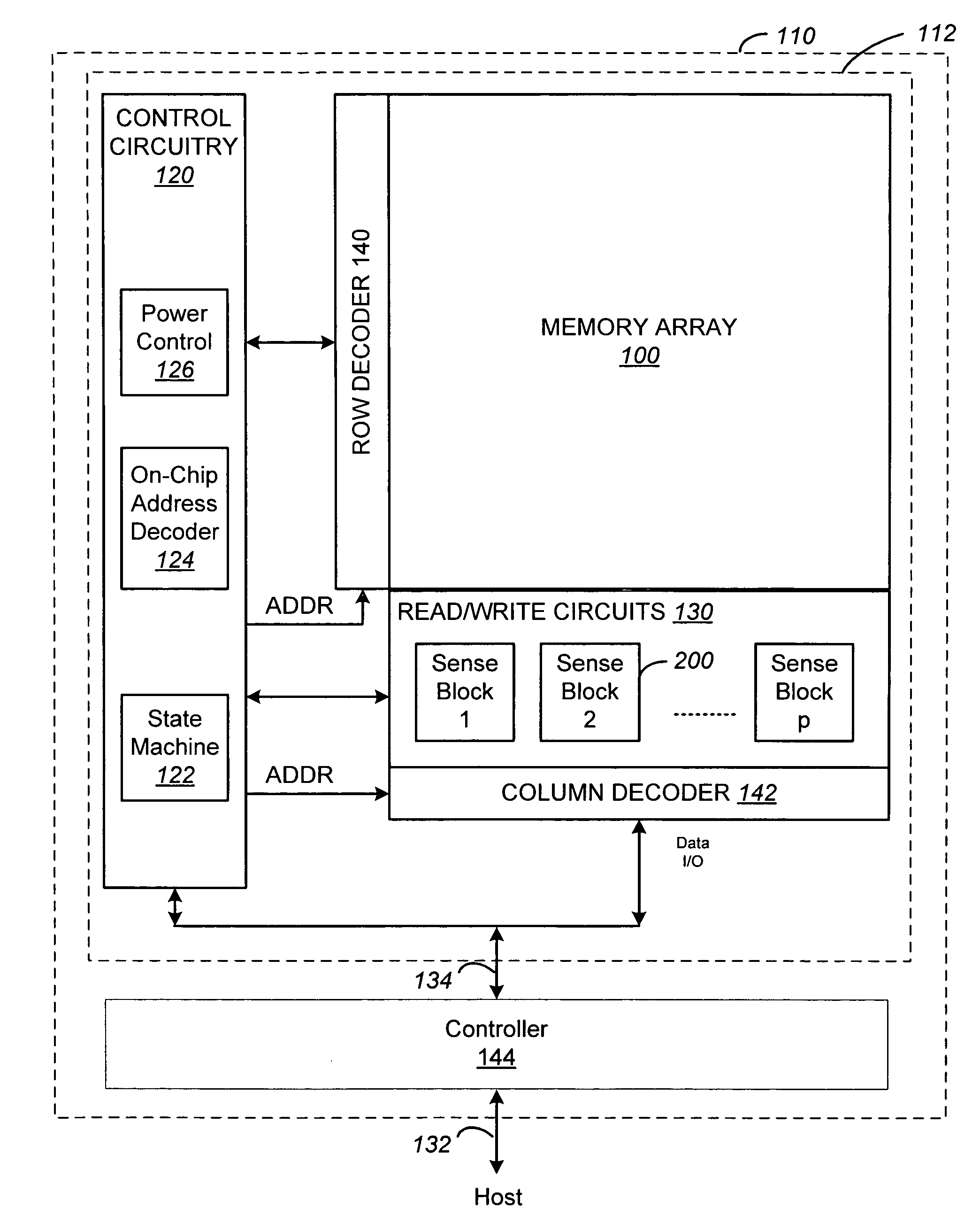
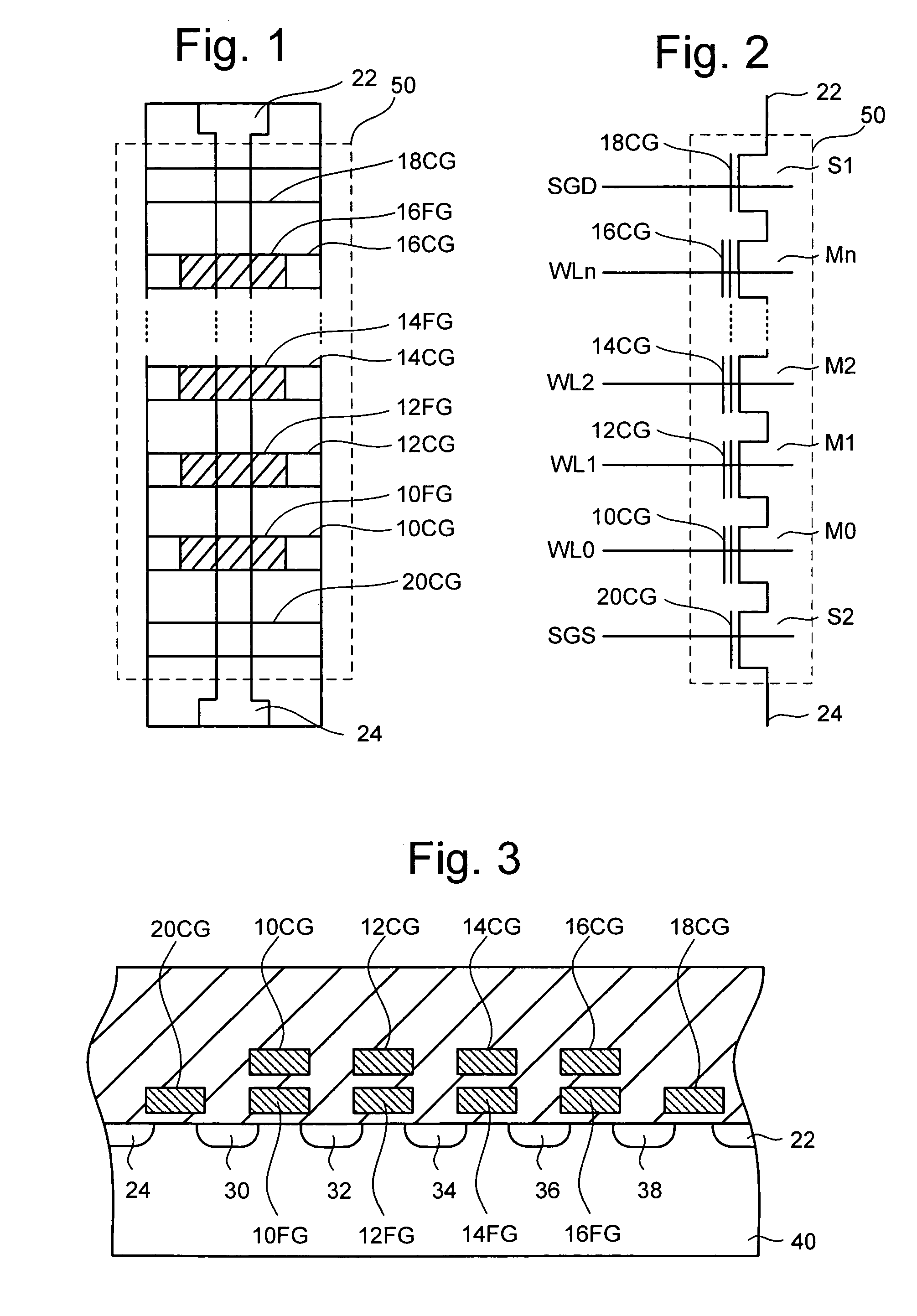
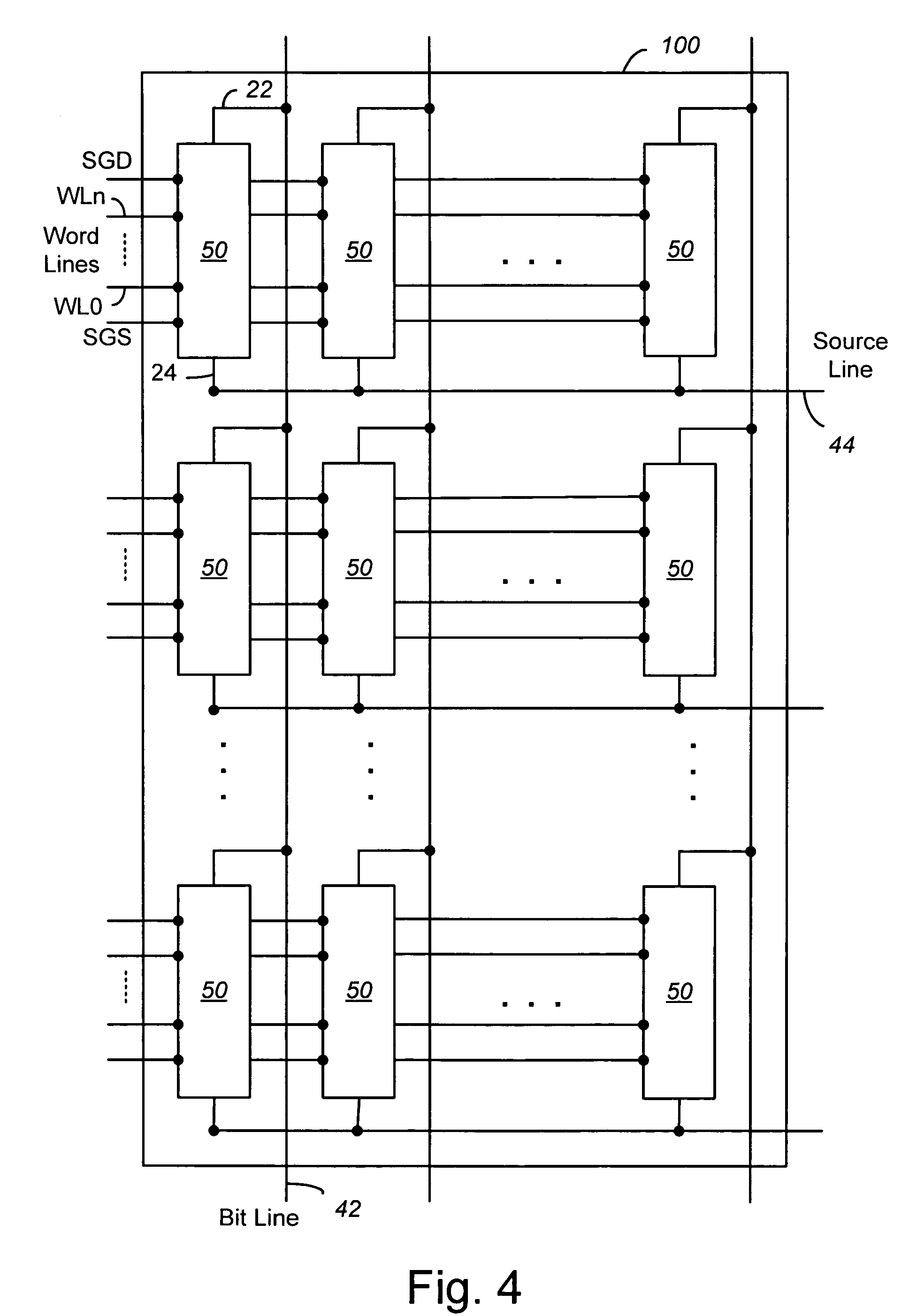
[0046] One example of a memory system suitable for implementing embodiments of the present invention uses the NAND flash memory structure, which includes arranging multiple transistors in series between two select gates. The transistors in series and the select gates are referred to as a NAND string. FIG. 1 is a top view showing an exemplary NAND string 50. FIG. 2 is an equivalent circuit thereof. The NAND string depicted in FIGS. 1 and 2 includes transistors, M0, M1, M2, and Mn, in series and sandwiched between a first select gate S1 and a second select gate S2. In one embodiment, transistors M0, M1, M2, and Mn each form an individual memory cell of the NAND string. In other embodiments, the memory cells of a NAND string may include multiple transistors or may be different than that depicted in FIGS. 1 and 2. The memory cell Mn is labeled as such to indicate that a NAND string can include any number (n) memory cells, be it less than or greater than four as depicted (e.g., 2, 8, 16,...


PUM


Abstract

Shifts in the apparent charge stored on a floating gate of a non-volatile memory cell can occur because of coupling of an electric field based on the charge stored in adjacent floating gates. The shift in apparent charge can lead to erroneous readings by raising the apparent threshold voltage, and consequently, lowering the sensed conduction current of a memory cell. The read process for a selected memory cell takes into account the state of one or more adjacent memory cells. If an adjacent memory cell is in one or more of a predetermined set of programmed states, a compensation current can be provided to increase the apparent conduction current of the selected memory cell. An initialization voltage is provided to the bit line of the programmed adjacent memory cell to induce a compensation current between the bit line of the programmed adjacent memory cell and the bit line of the selected memory cell.

Description

BACKGROUND OF THE INVENTION [0001] 1. Field of the Invention [0002] The present invention relates to technology for non-volatile memory. [0003] 2. Description of the Related Art [0004] Semiconductor memory has become more popular for use in various electronic devices. For example, non-volatile semiconductor memory is used in cellular telephones, digital cameras, personal digital assistants, mobile computing devices, non-mobile computing devices and other devices. Electrically Erasable Programmable Read Only Memory (EEPROM), including flash EEPROM, and Electrically Programmable Read Only Memory (EPROM) are among the most popular non-volatile semiconductor memories. [0005] EEPROM and EPROM are non-volatile memories that can be erased and have new data written or “programmed” into their memory cells. Both utilize a floating gate in a transistor structure that is positioned above and insulated from a channel region in a semiconductor substrate. The floating gate is positioned between th...

Claims


Application Information

Patent Timeline
IPC IPC(8): G11C11/34
CPCG11C7/02G11C16/26G11C11/5642G11C7/12G11C16/04
Inventor CERNEA, RAUL-ADRIAN
Owner SANDISK TECH LLC
Why Eureka
Try Eureka