Organic electroluminescent element and organic electroluminescent display device

a technology of electroluminescent elements and organic electroluminescent elements, which is applied in the direction of discharge tube luminescnet screens, natural mineral layered products, transportation and packaging, etc., can solve the problems of limited limitation of expansion of a region, and inability to achieve improvement in light emitting efficiency, etc., to achieve further high light emitting efficiency, and enhanced light emitting efficiency

Inactive Publication Date: 2006-12-28
SANYO ELECTRIC CO LTD
View PDF9 Cites 167 Cited by
  • Summary
  • Abstract
  • Description
  • Claims
  • Application Information

AI Technical Summary

Benefits of technology

[0010] An object of the present invention is to provide, in an organic EL element provided with at least two light emitting units, an organic EL element which can be driven at a low voltage, has a high light emitting efficiency, and can exhibit a desired emitting color, and an organic EL display device. <First Aspect>

Problems solved by technology

However, since movement of a carrier in an organic EL element undergoes restriction due to an energy barrier between an electrode and an organic thin film, and low carrier mobility in an organic thin film, improvement in a light emitting efficiency is limited.
However, when 3 or more of light emitting layers are laminated so that they are directly contacted, improvement in a light emitting efficiency is not obtained.
This is because there is a limitation on expansion of a region for recombining an electron and a hole, and a recombination region does not span 3 or more layers.
For this reason, a driving voltage becomes high and this cannot be applied to low voltage driving of a portable equipment.

Method used


Image

  • Organic electroluminescent element and organic electroluminescent display device
  • Organic electroluminescent element and organic electroluminescent display device
  • Organic electroluminescent element and organic electroluminescent display device

Examples


experiment 1

Examples 1 to 5 and Comparative Examples 1 to 2

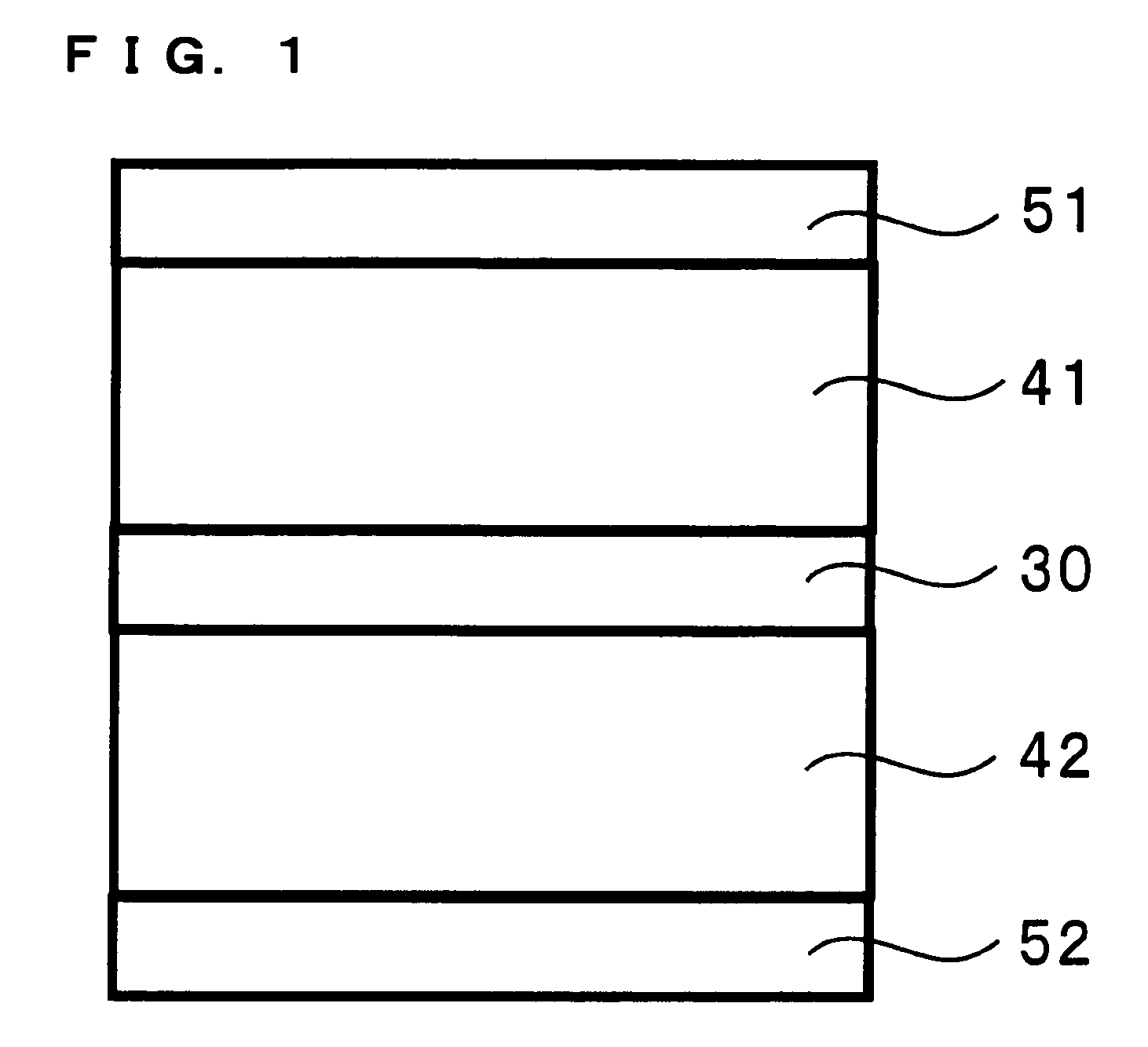
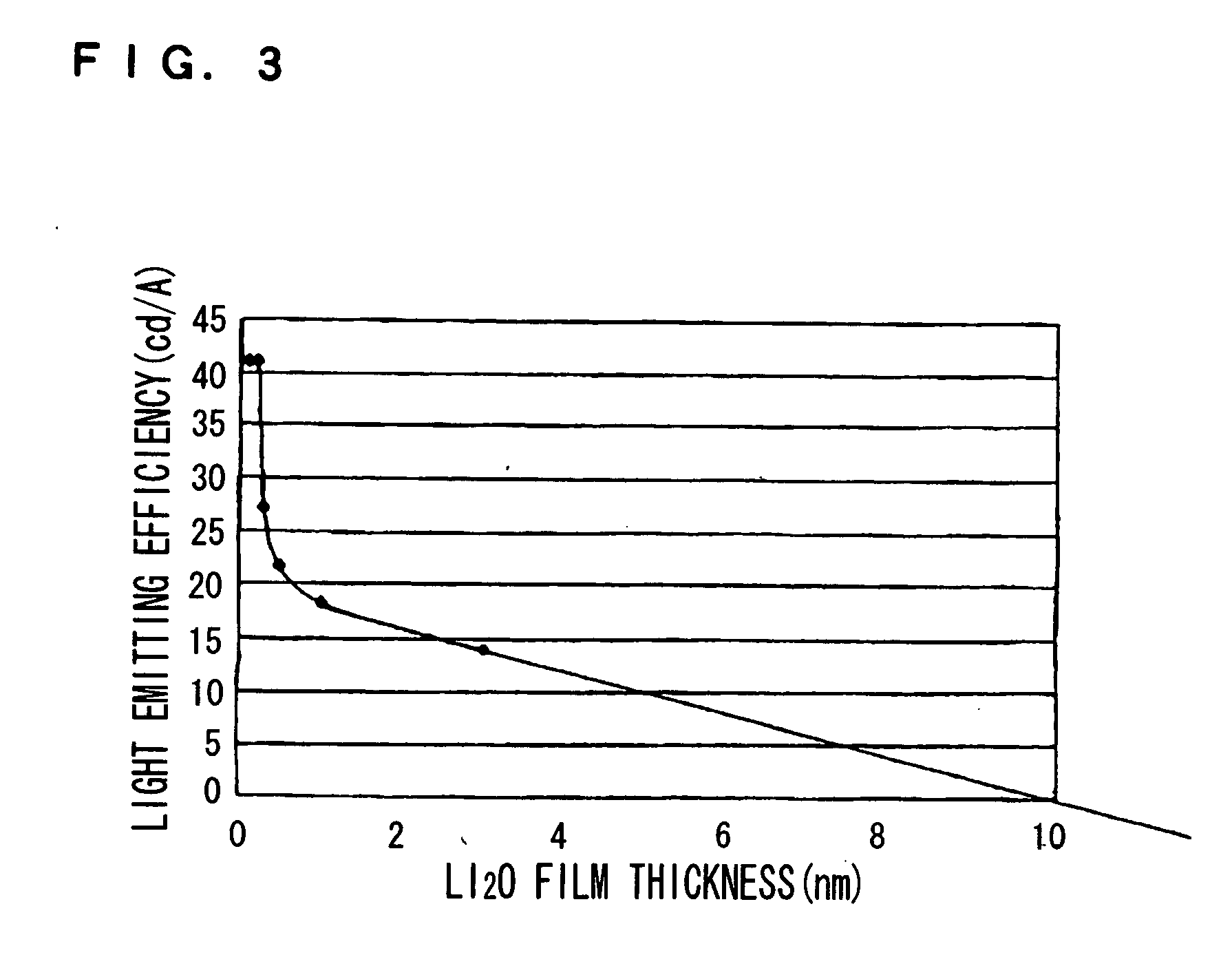
[0141] Organic EL elements of Examples 1 to 5 and Comparative Examples 1 to 2 having an anode, a hole injecting layer, a second light emitting unit, an intermediate unit, a first light emitting unit, an electron transporting layer, and a cathode shown in Table 1 were manufactured. In the following Table, a numerical in ( ) indicates a thickness (nm) of each layer.

[0142] An anode was manufactured by forming a fluorocarbon (CFx) layer on a glass substrate on which an ITO (indium tin oxide) film had been formed. A fluorocarbon layer was formed by plasma polymerization of a CHF3 gas. A thickness of a fluorocarbon layer was 1 nm.

[0143] On the thus manufactured anode, a hole injecting layer, a second light emitting unit, an intermediate unit, a first light emitting unit, an electron transporting layer, and a cathode were formed by successively depositing them by a deposition method.

[0144] A hole injecting layer was formed from HAT-CN6.

[0...

experiment 2

Example 6 and Comparative Example 3

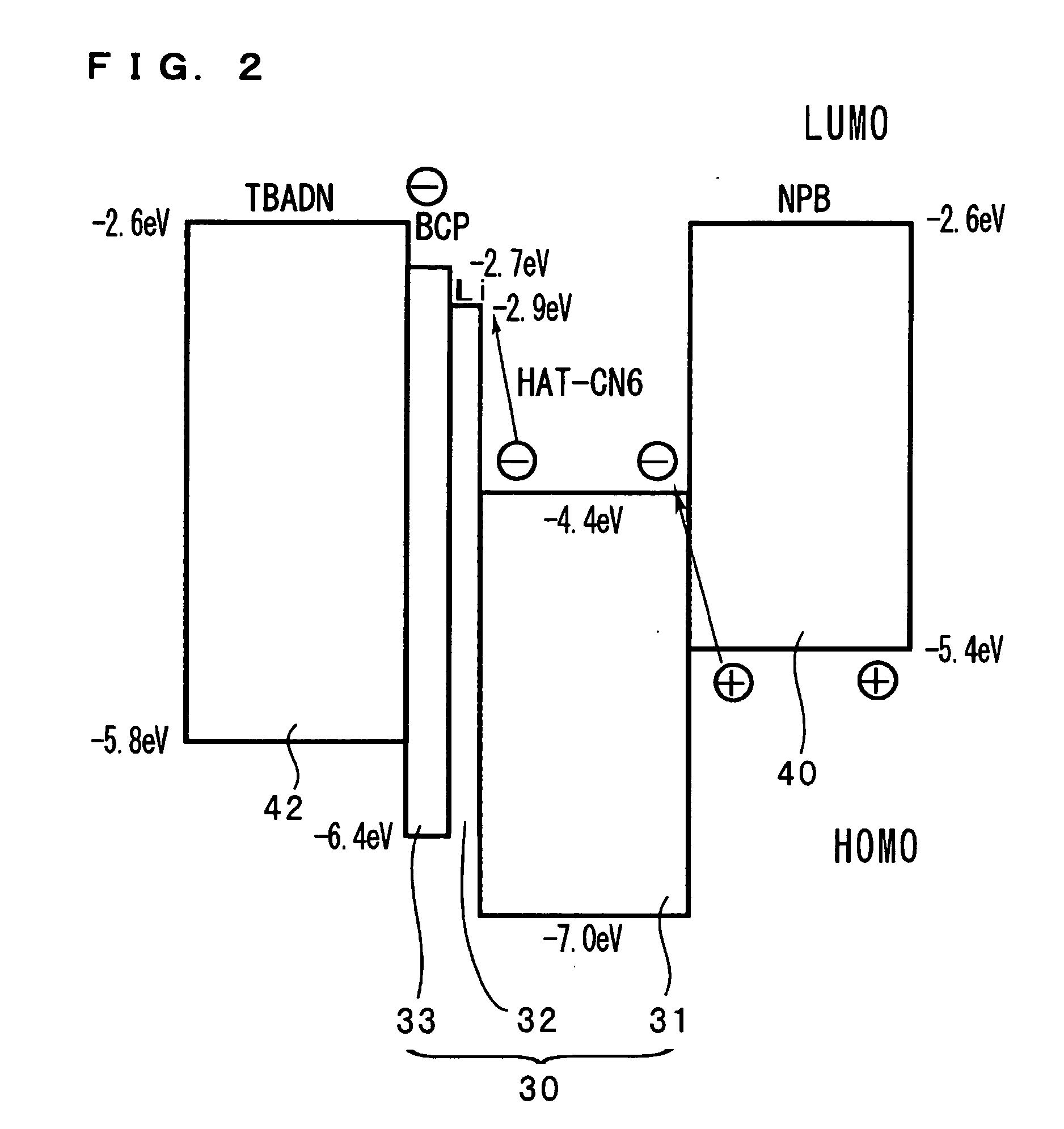
[0158] An organic EL element of Example 6 provided with an anode, a hole injecting layer, a second light emitting unit, an intermediate unit, a first light emitting unit, an electron transporting layer, and a cathode shown in Table 3 was manufactured as in the aforementioned Experiment 1. In addition, an organic EL element of Comparative Example 3 of a structure shown in Table 3, which is the same as the organic EL element of Example 4 except that an intermediate unit and a first light emitting unit were not possessed, was manufactured.

[0159] In the present Example, an adjacent layer comprising NPB is formed between a “HAT-CN6” layer of an intermediate unit, and a first light emitting unit. In addition, in the present Example, a first light emitting unit and a second light emitting unit are constructed of a blue single light emitting layer. Like this, when an arylamine-based hole transporting material such as NPB is not used as a host material in...

experiment 3

[0162] An organic EL element of Example 7 having an anode, a hole injecting layer, a second light emitting unit, an intermediate unit, a first light emitting unit, an electron transporting layer, and a cathode shown in Table 5 was manufactured as in the Experiment 1.

[0163] In the present Example, as a first light emitting unit and a second light emitting unit, the same blue single light emitting layer as that of Example 1 is used. In addition, in the present Example, an adjacent layer comprising TPD is provided in an intermediate unit. A hole transporting layer comprising NPB is provided between this adjacent layer comprising TPD, and a first light emitting unit.

[0164] In addition, in the present Example, TPD is used also in a hole injecting layer provided between an anode and a second light emitting unit. As shown in Table 5, a layer comprising TPD is provided between a “HAT-CN6” layer and a NPB layer.

[0165] TPD is N,N′-bis-(3-methylphenyl) -N,N′-bis-(phenyl)-benzidine, and has ...


PUM

PropertyMeasurementUnit
thicknessaaaaaaaaaa
thicknessaaaaaaaaaa
thicknessesaaaaaaaaaa

Abstract

An organic electroluminescent element comprising a cathode, an anode, an intermediate unit arranged between a cathode and an anode, a first light emitting unit arranged between a cathode and an intermediate unit, and a second light emitting unit arranged between an anode and an intermediate unit, wherein an electron extracting layer for extracting an electron from an adjacent layer adjoining a cathode side is provided in an intermediate unit, an absolute value of an energy level of a lowest unoccupied molecular orbital (LUMO) of an electron extracting layer |LUMO(A)|, and an absolute value of an energy level of a highest occupied molecular orbital (HOMO) of the adjacent layer |HOMO(B)| are in the relationship of |HOMO(B)|−|LUMO(A)|≦1.5 eV, and an intermediate unit supplies a hole generated by extraction of an electron from an adjacent layer by an electron extracting layer and, at the same time, supplies the extracted electron to a second light emitting unit.

Description

[0001] The priority Japanese Patent Application Numbers 2004-224905, 2004-224906, 2004-224907, 2004-224908, 2004-224909, 2004-224910, 2004-347296, 2005-024212, 2005-050034 and 2005-050035 upon which this patent application is based is hereby incorporated by reference. BACKGROUND OF THE INVENTION [0002] 1. Field of the Invention [0003] The present invention relates to an organic electroluminescent element and an organic electroluminescent display device. [0004] 2. Description of the Related Art [0005] An organic electroluminescent element (organic EL element) has been actively developed from a viewpoint of application to display and illumination. Principle for driving an organic EL element is as follows; That is, a hole and an electron are injected through an anode and a cathode, respectively, these are transported in an organic thin film, and recombined in a light emitting layer to generate the excited state, and light emitting is obtained from this excited state. In order to enhanc...

Claims


Application Information

Patent Timeline
Patent Type & Authority Applications(United States)
IPC IPC(8): H01L51/54H05B33/00
CPCC09K11/06Y10T428/24116C09K2211/1011C09K2211/1037H01L27/3248H01L51/0051H01L51/0054H01L51/0065H01L51/0068H01L51/0072H01L51/5036H01L51/5278H01L2251/5315H01L2251/552H01L2251/558H05B33/14C09K2211/1007H10K59/123H10K85/611H10K85/622H10K85/653H10K85/655H10K85/6572H10K50/125H10K50/19H10K2102/3026H10K2101/30H10K2102/351
Inventor NISHIMURA, KAZUKIHAMADA, YUJIIYORI, MASAHIROHASHIMOTO, HARUHISASAKATA, MASAKAZUIZUMI, HIROAKIITO, KANAMEISHIKAWA, KAORIISHIDA, HIROKI
Owner SANYO ELECTRIC CO LTD
Why Eureka
Try Eureka