Structure improvement of depletion region in p-i-n photodiode

a photodiode and depletion region technology, applied in the direction of basic electric elements, electrical equipment, semiconductor devices, etc., can solve the problems of slowing down the transmission speed of electrons, affecting the efficiency of photodetectors, so as to improve the output power and bandwidth of photodetectors, and prevent the drifting velocity of electrons

Inactive Publication Date: 2006-12-28
NAT CENT UNIV
View PDF3 Cites 8 Cited by
  • Summary
  • Abstract
  • Description
  • Claims
  • Application Information

AI Technical Summary

Benefits of technology

[0008] Therefore, the main purpose of the present invention is to improve the product of output power and bandwidth of a photodetector and to prevent the drifting velocity of electron from slowing down under a high bias, which can be applied to a photodetector of communicative wave length over optical fiber.

Problems solved by technology

When a traditional p-i-n photodiode is put under an irradiation using a high optical power, the speed performance becomes worse and the maximum electric output power becomes lower than usual because the added electric field is shielded by the space electric field reacted by inner photo-excited carriers.
But, when operated under a high power, a great deal of photocurrent will pass by a load resistance and produce an electric field with a polarity opposite to the bias added to the optical detector.
Nevertheless, the high bias will slow down the transmitting velocity of electrons, accompanying by a trade-off among velocity, efficiency and maximum power concerning area size, and also accompanying by a trade-off between the maximum output current and the breakdown voltage in a doped collector layer.
So, the moving velocities of photo-excited carriers in this area are greatly lowered to greatly worsen the velocity performance of the whole structure and limit the output power.
But, the velocity of a large component will be seriously limited by the RC (resistance-capacitance) delay time so that, even though a UTC structure can successfully imp roves the product of the power and the bandwidth a trade-off between the maximum output power (and efficiency) and the bandwidth concerning are a size still exists.

Method used


Image

  • Structure improvement of depletion region in p-i-n photodiode
  • Structure improvement of depletion region in p-i-n photodiode
  • Structure improvement of depletion region in p-i-n photodiode

Examples


Embodiment Construction

[0023] The following descriptions of the preferred embodiments are provided to understand the features and the structures of the present invention.

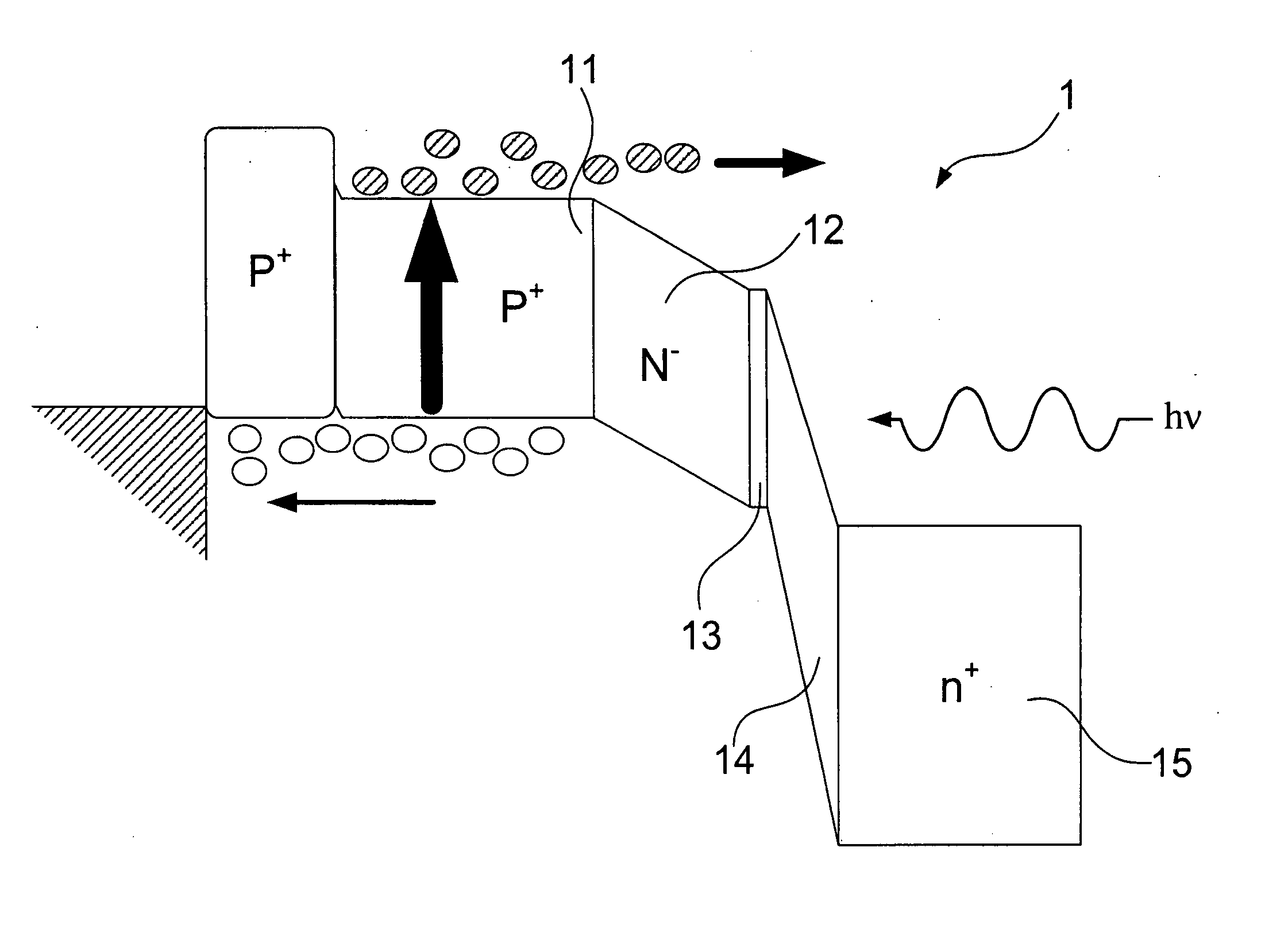
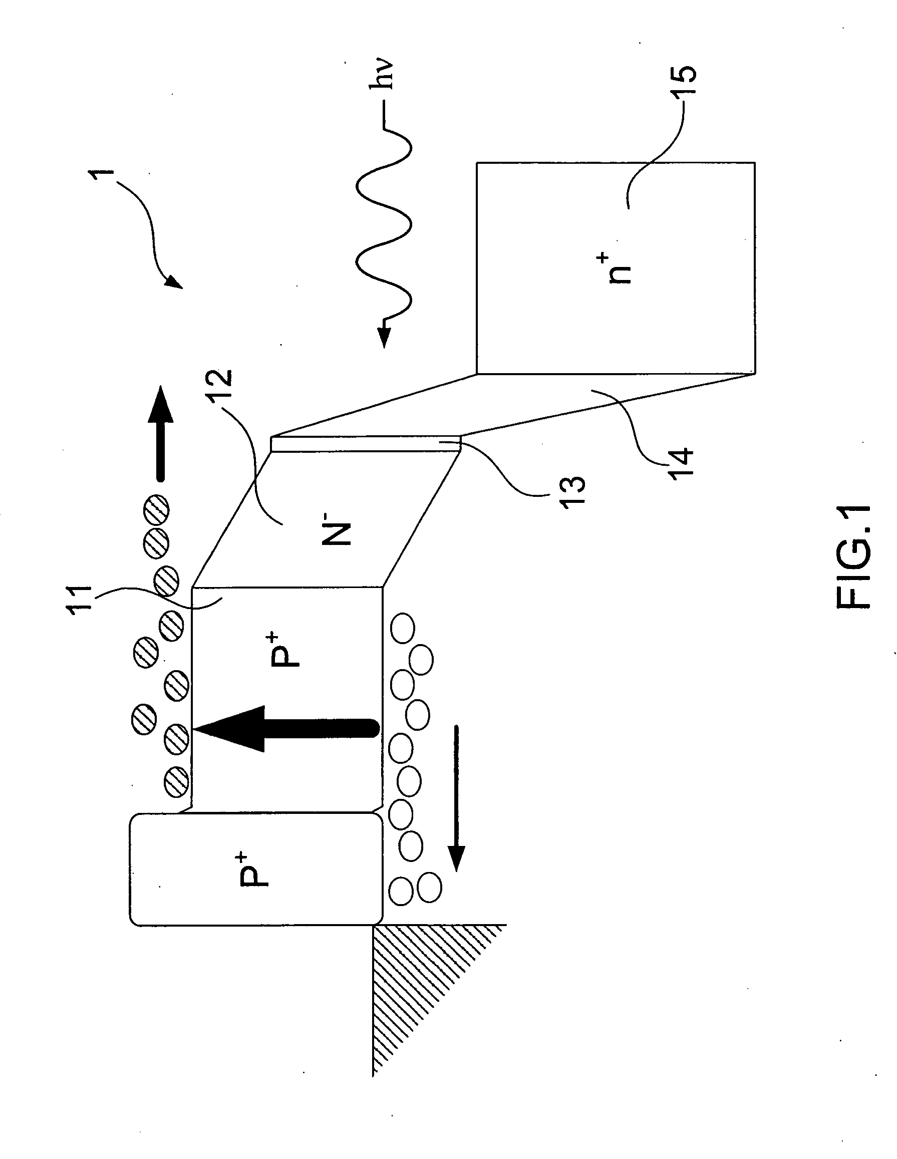
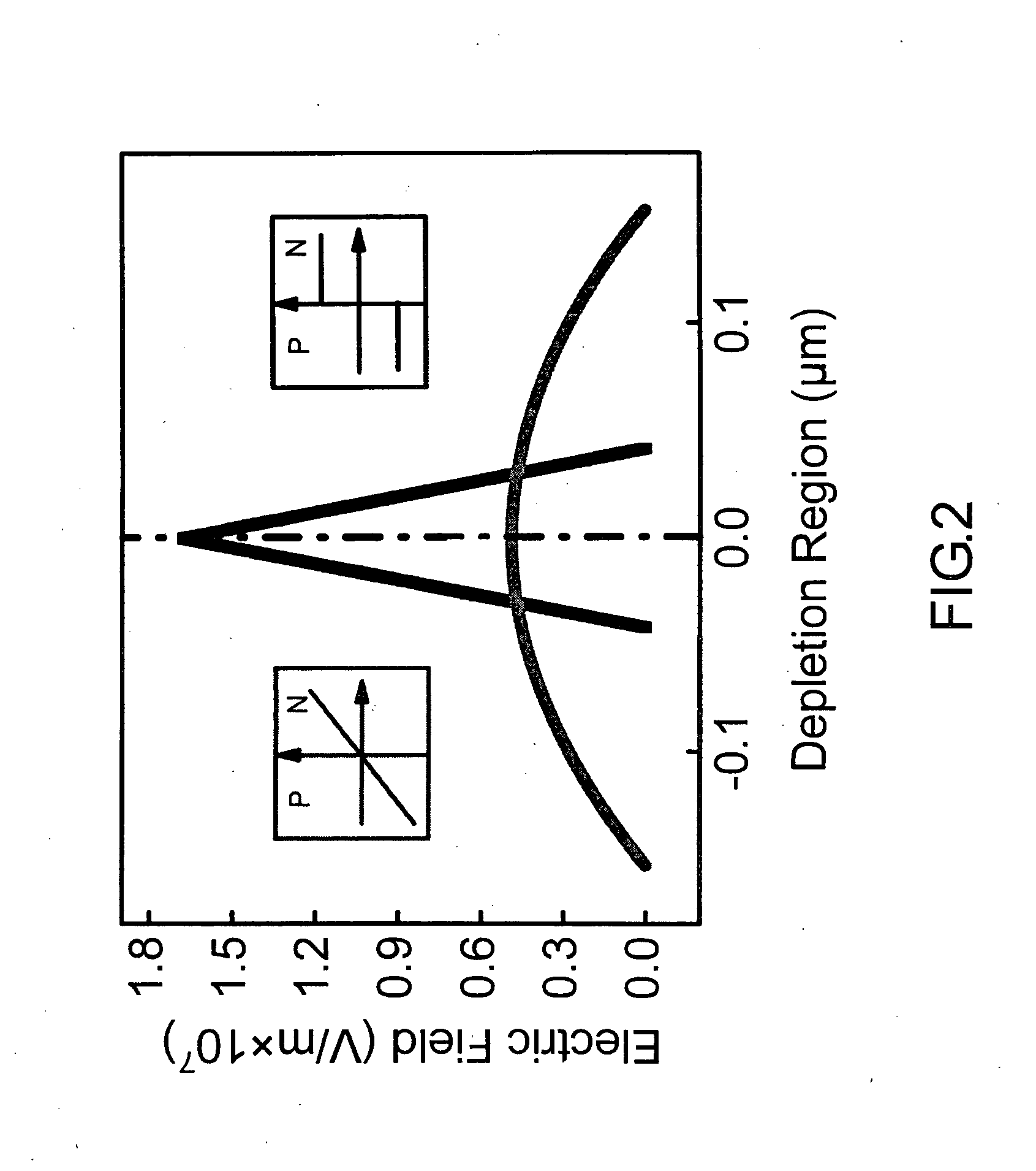
[0024] Please refer to FIG. 1, which is a structural view according to the present invention. As shown in the figure, the present invention is a structure improvement of depletion region in a p-i-n photodiode, where its epitaxy layer 1 comprises a first p-type doped layer 11, a first n-type doped layer 12, a second p-type doped layer 13, an undoped layer 14, and a second n-type doped layer 15, to form a p-n-p-i-n epitaxy layer grown on any doped diode or semi-insulated diode made of GaAs, InP, GaN, AlN, Si or GaSb. The first p-type doped layer 11 is made of a light-absorbing material to be a light-absorbing layer; and, is graded doped to accelerate electron discharge. The first n-type doped layer 12 is made of a material of ballistic transmission to accelerate the transmission of carrier; and, is graded doped to increase a breakdown volt...


PUM


Abstract

The present invention with a structure of depletion region improves the product of output power and bandwidth of a photodetector and prevents the drifting velocity of electron from slowing down under a bias, which can be applied to a photodetector of communicative wavelength over optical fiber.

Description

FIELD OF THE INVENTION [0001] The present invention relates to a structure of depletion region; more particularly, relates to improving the product of output power and bandwidth of a photodetector and preventing the drifting velocity of electron from slowing down under a high bias. DESCRIPTION OF THE RELATED ART [0002] In the development of high-speed photodetector, one of the key targets is the product of output power and bandwidth. When a traditional p-i-n photodiode is put under an irradiation using a high optical power, the speed performance becomes worse and the maximum electric output power becomes lower than usual because the added electric field is shielded by the space electric field reacted by inner photo-excited carriers. Hence, then, a Uni-traveling Carrier Photodetector (UTC-PD) is provided, where the light-absorbing material of InP. With p-i-n photodiode is changed from the i-layer to a p-type doped layer and the original i-layer is substituted with a non light-absorbi...

Claims


Application Information

Patent Timeline
Patent Type & Authority Applications(United States)
IPC IPC(8): H01L29/221
CPCH01L31/105
Inventor WU, YEN-HSIANG
Owner NAT CENT UNIV
Why Eureka
Try Eureka