
Surge absorption circuit

Active Publication Date: 2006-12-28
TDK CORPARATION
View PDF10 Cites 5 Cited by
  • Summary
  • Abstract
  • Description
  • Claims
  • Application Information

AI Technical Summary

Benefits of technology

[0018] It is an object of the present invention to provide a surge absorption circuit which is excellent in impedance matching with respect to high-speed differential signals of differential inputs as well.
[0019] A surge absorption circuit in accordance with the present invention cancels the influence of the stray capacitance component of a surge absorbing device by utilizing an inductor device.
[0023] Accordingly, the present invention can provide a surge absorption circuit which is excellent in impedance matching with respect to high-speed differential signals as well while protecting semiconductor devices and the like against high-voltage static electricity.
[0027] Connecting the resistor device or inductor device in series to the surge absorbing device can cancel the equivalent parallel resistance component or equivalent parallel capacitance component of the inductor device in the case of differential signals, thereby realizing a flat frequency characteristic over a wide band.
[0031] Connecting a resistor device or capacitor device in parallel to the inductor device can cancel the influence of the equivalent series resistance component or equivalent series inductance component of the surge absorbing device in the case of differential signals, thereby realizing a flat frequency characteristic over a wide band.
[0034] The inductive coupling can eliminate common-mode noise, and can realize a flat frequency characteristic over a wide band in the case of differential signals.

Problems solved by technology

However, even the circuit shown in FIG. 5 cannot realize a sufficient characteristic.
Since the conditions of expression (2-1) and expression (2-2) exists, however, it is not possible to match the input impedance to the characteristic impedance at high frequencies.

Method used


Image

  • Surge absorption circuit
  • Surge absorption circuit
  • Surge absorption circuit

Examples


first embodiment

[0061] First Embodiment

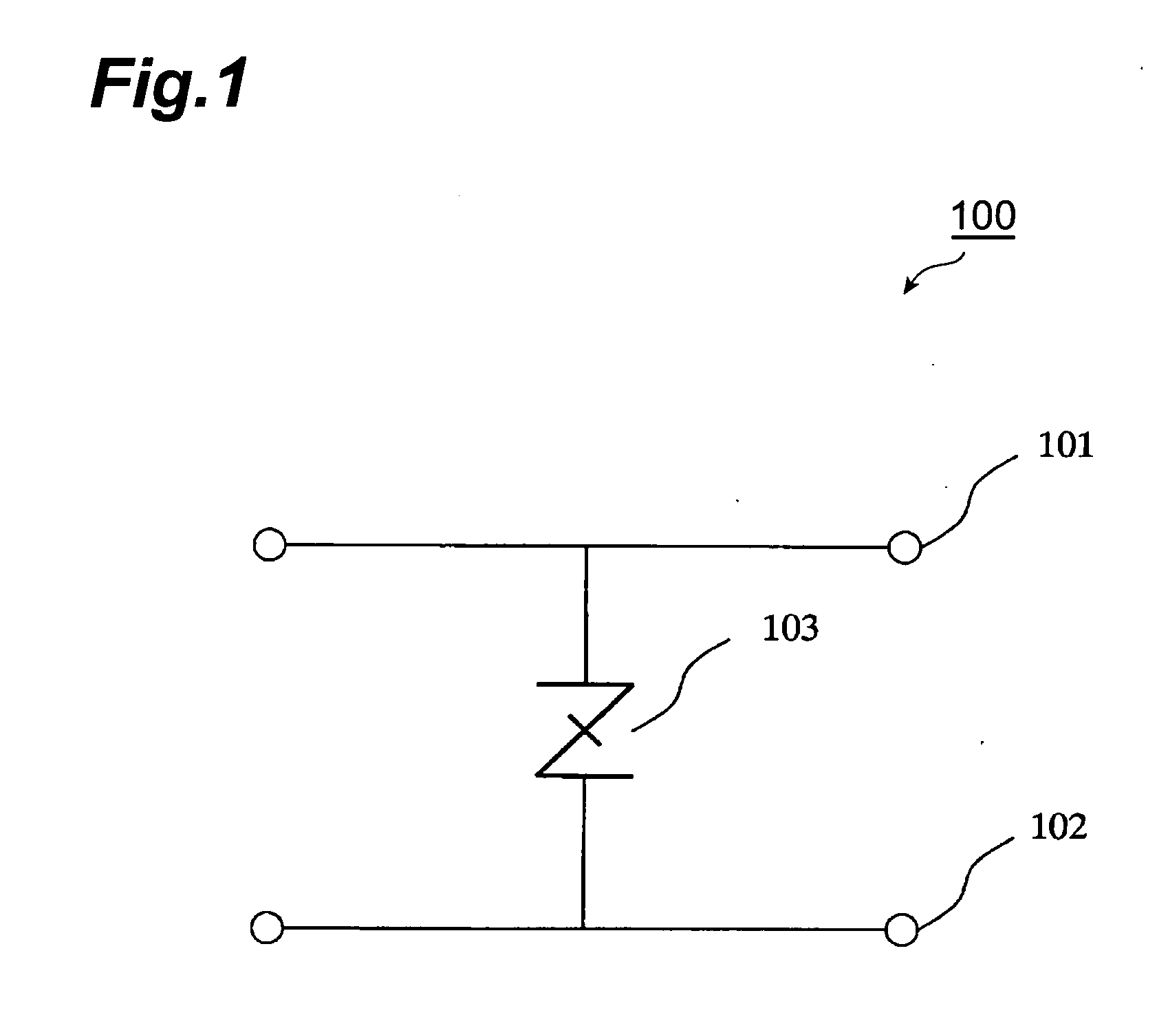
[0062]FIG. 7 shows the circuit structure of the surge absorption circuit in accordance with an embodiment of the present invention. A surge absorption circuit 10 shown in FIG. 7 comprises one input terminal 11 of differential input terminals, the other input terminal 12 of the differential input terminals, one output terminal 13 of differential output terminals, the other output terminal 14 of the differential output terminals, a first surge absorbing device 21, a second surge absorbing device 22, a first inductor device 25, and a second inductor device 26.

[0063] As shown in FIG. 7, the surge absorption circuit 10 comprises a pair of input terminals 11 and 12 and a pair of output terminals 13 and 14 for connection to the outside. The first inductor device 25 is connected between the input terminal 11 and output terminal 13, whereas the second inductor device 26 is connected between the input terminal 12 and output terminal 14. The first surge absorbing device...

second embodiment

[0090] Second Embodiment

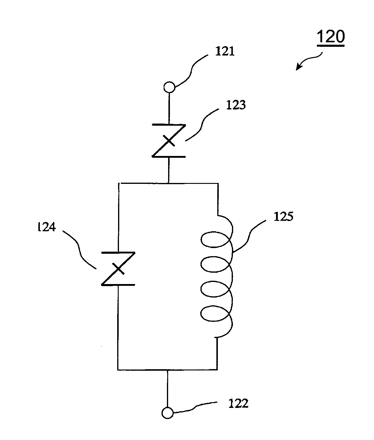
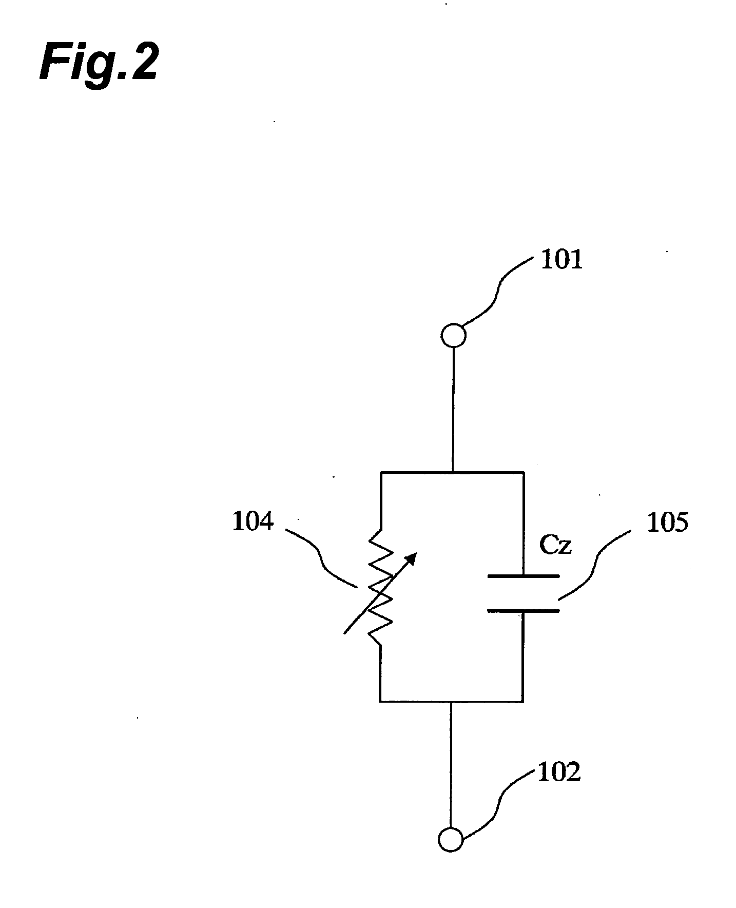
[0091]FIG. 16 shows the circuit structure of the surge absorption circuit in accordance with an embodiment of the present invention. A surge absorption circuit 20 shown in FIG. 16, one input terminal 11 of differential input terminals, the other input terminal 12 of the differential input terminals, one output terminal 13 of differential output terminals, the other output terminal 14 of the differential output terminals, a first surge absorbing device 21, a second surge absorbing device 22, a first inductor device 25, a second inductor device 26, a third resistor device 35, a fourth resistor device 36, a first capacitor device 37, and a second capacitor device 38.

[0092] The surge absorption circuit shown in FIG. 16 has such a structure that the third resistor device 35 and first capacitor device 37 connected in parallel between the input terminal 11 and output terminal 13 and the fourth resistor device 36 and second capacitor device 38 connected in parallel ...

third embodiment

[0106] Third Embodiment

[0107]FIG. 19 shows the circuit structure of the surge absorption circuit in accordance with an embodiment of the present invention. The surge absorption circuit 30 shown in FIG. 19 comprises: one input terminal 11 of differential input terminals; the other input terminal 12 of the differential input terminals; one output terminal 13 of differential output terminals; the other output terminal 14 of the differential output terminals; a first surge absorbing device 21; a second surge absorbing device 22; a first inductor device 25; a second inductor device 26; a first resistor device 31; a second resistor device 32; a third inductor device 33, and a fourth inductor device 34. In the surge absorption circuit 30, the first surge absorbing device 21, the first resistor device 31 and the third inductor device 33 are connected in series, thereby configuring the first surge absorbing portion. In addition, the second surge absorbing device 22, the second resistor devic...


PUM


Abstract

A surge absorption circuit in accordance with an embodiment comprises: a pair of input terminals; a pair of output terminals; a first inductor device connecting one of the pair of input terminals and one of the pair of output terminals to each other; a second inductor device connecting the other of the pair of input terminals and the other of the pair of output terminals to each other; a first surge absorption part having a first surge absorbing device and connected in series between the one of the pair of input terminals and the other of the pair of output terminals; and a second surge absorption part having a second surge absorbing device and connected in series between the other of the pair of input terminals and the one of the pair of output terminals.

Description

BACKGROUND OF THE INVENTION [0001] 1. Field of the Invention [0002] The present invention relates to a surge absorption circuit with an improved high-frequency characteristic. [0003] 2. Related Background of the Invention [0004] Since semiconductor devices such as IC and LSI are destroyed or caused to deteriorate their properties by high-voltage static electricity, surge absorbing devices such as varistors have been in use as measures against static electricity. The surge absorbing devices such as varistors have a stray capacitance component and an equivalent series inductance component, and thus deteriorate signals when employed in circuits dealing with high-speed signals. [0005]FIG. 1 is a diagram showing an example in which a varistor is employed in a surge absorption circuit. A surge absorption circuit 100 shown in FIG. 1 comprises an I / O terminal 101, a common terminal 102, and a varistor 103. When an input signal having a small amplitude is fed to the I / O terminal 101, the var...

Claims


Application Information

Patent Timeline
IPC IPC(8): H02H9/06
CPCH01F17/0006H01F27/40H03H7/09H03H7/0107H03H7/38H03H2001/0085H03H7/1766H02H9/04H03H5/12
Inventor TERADA, YUJI
Owner TDK CORPARATION
Features
  • Generate Ideas
  • Intellectual Property
  • Life Sciences
  • Materials
  • Tech Scout
  • Unparalleled Data Quality
  • Higher Quality Content
  • 60% Fewer Hallucinations
Learn More