

Non-volatile memory, manufacturing and operating method thereof
a technology of non-volatile memory and manufacturing method, applied in semiconductor devices, digital storage, instruments, etc., can solve problems such as difficult to achieve a high level of integration, data read-out errors may occur, and presence of net positive charge, so as to achieve high electron injection efficiency, reduce memory cell current, and increase operating speed
- Summary
- Abstract
- Description
- Claims
- Application Information
AI Technical Summary
Benefits of technology
Problems solved by technology
Method used
Image

Examples
Embodiment Construction
[0051] Reference will now be made in detail to the present embodiments of the invention, examples of which are illustrated in the accompanying drawings. Wherever possible, the same reference numbers are used in the drawings and in the description to refer to the same or similar parts.
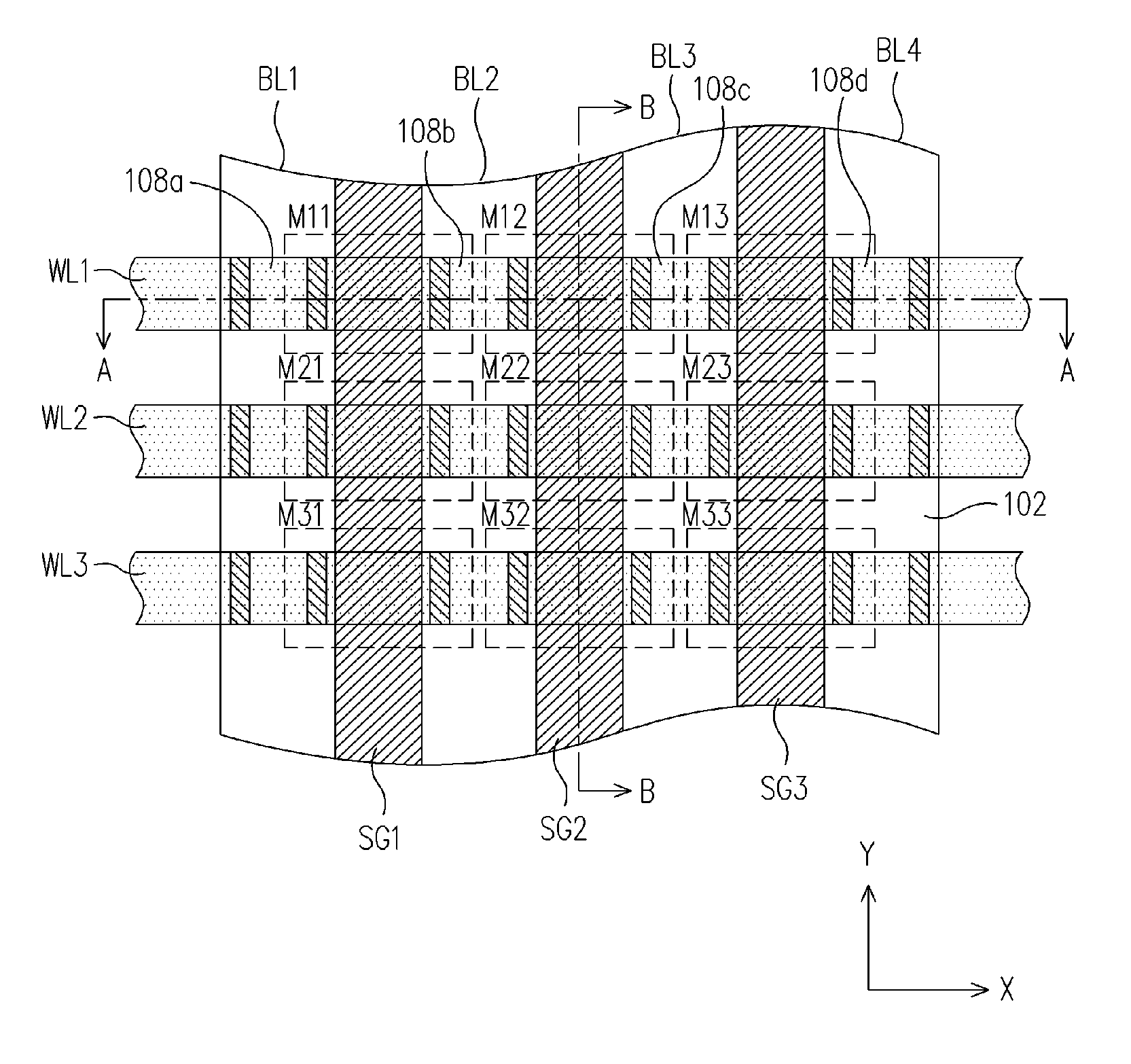
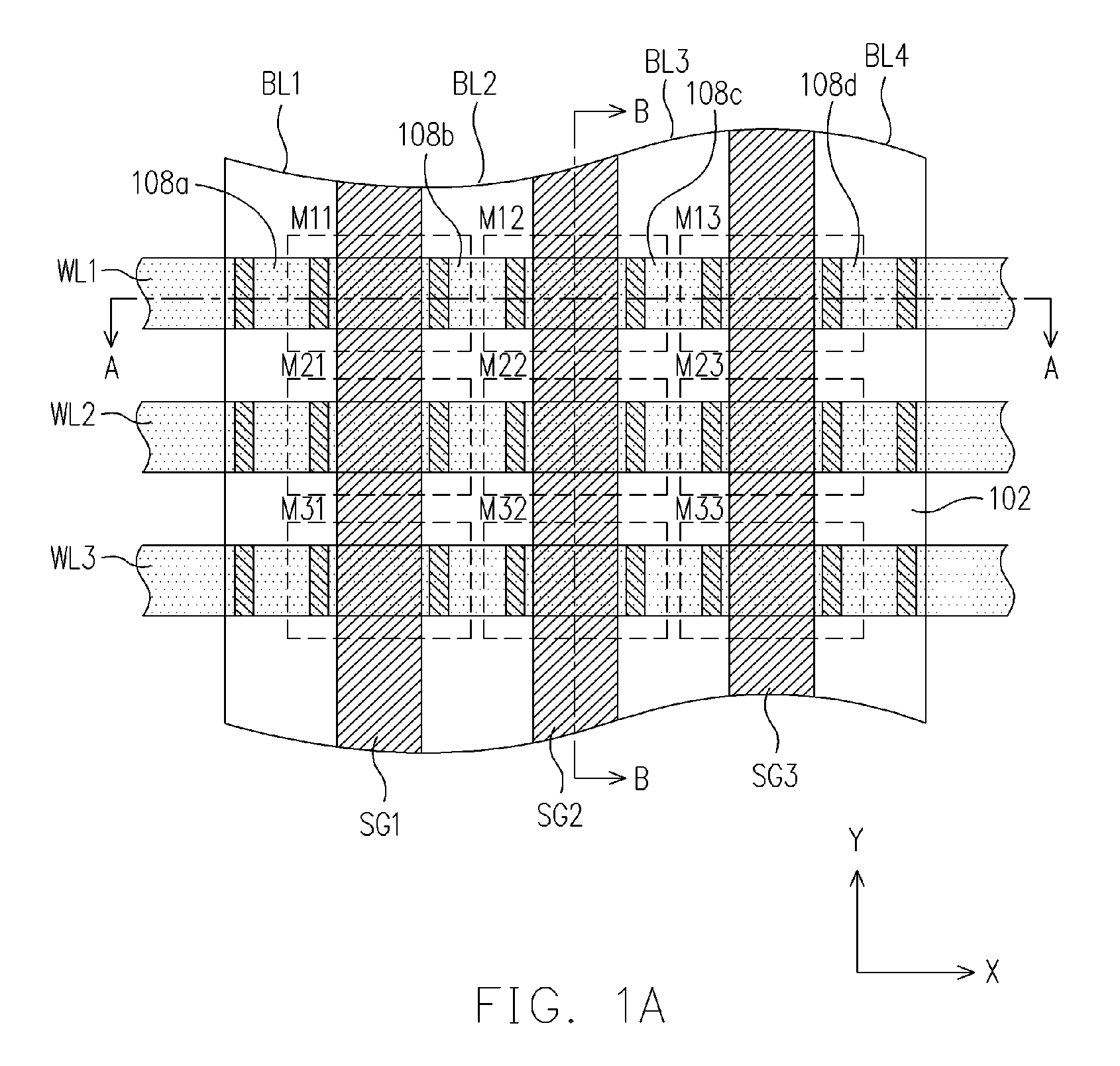
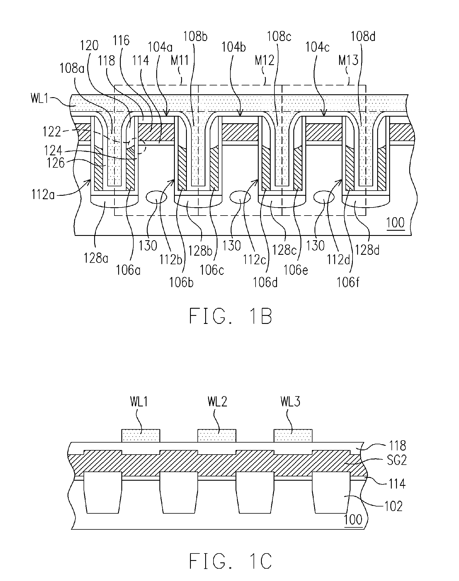
[0052]FIG. 1A is a top view of a non-volatile memory according to one embodiment of the present invention. FIG. 1B is a schematic cross-sectional view along line A-A′ of FIG. 1A. FIG. 1C is a schematic cross-sectional view along line B-B′ of FIG. 1A.
[0053] As shown in FIG. 1A, the non-volatile memory array in the present invention includes a substrate 100, a plurality of memory cells M11˜M33, a plurality of word lines WL1˜WL3, a plurality of select gate lines SG1˜SG3, and a plurality of bit lines BL1˜BL4.
[0054] The substrate 100 is a silicon substrate, for example. The substrate 100 has a plurality of embedded device isolation structures 102 to define active regions. The device isolation structures 1...
PUM
 Abstract
Description
Claims
Application Information