Heat treatment apparatus of light emission type

a heat treatment apparatus and light emission technology, applied in the direction of drying machines, light and heating apparatus, drying, etc., can solve the problems of poor uniform the impedance to good device formation, and the non-uniformity of the within-wafer illuminance distribution, so as to improve the within-wafer uniformity of the temperature distribution of the substrate, improve the workability, and improve the effect of the within-wa

Inactive Publication Date: 2006-12-28
DAINIPPON SCREEN MTG CO LTD
View PDF3 Cites 19 Cited by
  • Summary
  • Abstract
  • Description
  • Claims
  • Application Information

AI Technical Summary

Benefits of technology

[0012] The heat treatment apparatus is capable of increasing the temperature of part of a substrate peripheral portion close to the above-mentioned edge portion when the substrate is exposed to the flash of light to improve the within-wafer uniformity of a temperature distribution of the substrate during the heat treatment, especially the temperature distribution uniformity in the substrate peripheral portion.
[0014] The heat treatment apparatus is capable of increasing the temperature of the part of the substrate peripheral portion having the relatively low temperature to improve the temperature distribution uniformity in the substrate peripheral portion.
[0016] The heat treatment apparatus is capable of increasing the temperature of parts of a substrate peripheral portion close to edge portions of the opening of the clamp member which are located on the minor axis thereof when the substrate is exposed to the flash of light to improve the within-wafer uniformity of a temperature distribution of the substrate during the heat treatment, especially the temperature distribution uniformity in the substrate peripheral portion. Additionally, the clamp member has good workability.
[0017] It is therefore an object of the present invention to provide a heat treatment apparatus capable of improving the within-wafer uniformity of a temperature distribution of a substrate during heat treatment, especially the temperature distribution uniformity in a substrate peripheral portion.

Problems solved by technology

The occurrence of such a phenomenon causes the depth of the junction to exceed a required level, giving rise to an apprehension about a hindrance to good device formation.
In particular, a wafer having a diameter as large as 300 mm exhibits a large degree of lowering in illuminance in the peripheral portion thereof to result in the poor uniformity of a within-wafer illuminance distribution.
However, it has been found that a heat treatment apparatus employing a xenon flash lamp presents not only the non-uniformity of a temperature distribution in a radial direction of the semiconductor wafer but also the non-uniformity of a temperature distribution in a circumferential direction of the semiconductor wafer having the same radius.
For elimination of such non-uniformity of the temperature distributions, it is impossible to adjust the light source of the xenon flash lamp.
It is also difficult for a hot plate for preheating the semiconductor wafer prior to the flash heating to eliminate the non-uniformity of the temperature distribution in the circumferential direction of the semiconductor wafer having the same radius.

Method used


Image

  • Heat treatment apparatus of light emission type
  • Heat treatment apparatus of light emission type
  • Heat treatment apparatus of light emission type

Examples


Embodiment Construction

[0030] A preferred embodiment according to the present invention will now be described in detail with reference to the drawings.

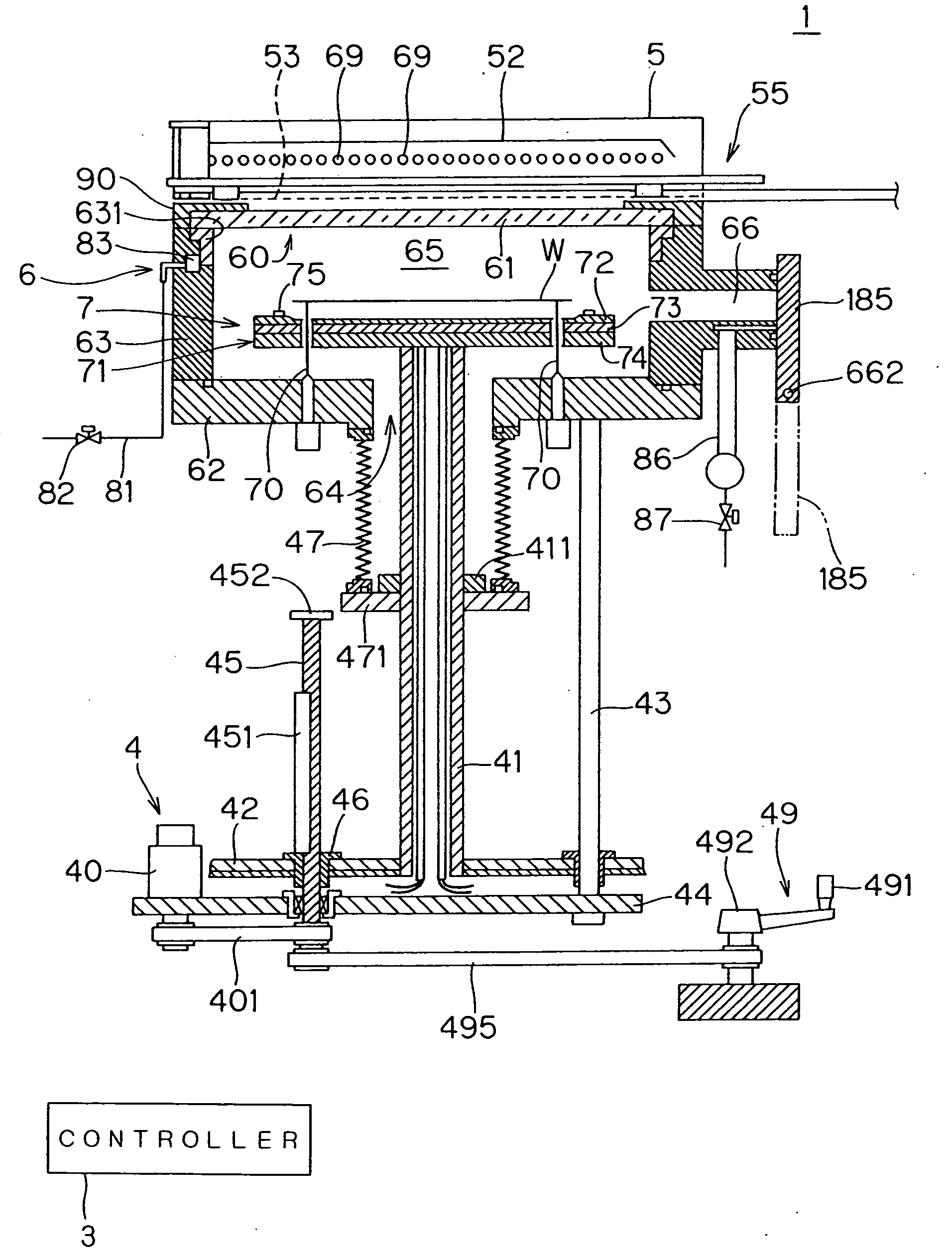
[0031] First, the overall construction of a heat treatment apparatus according to the present invention will be outlined. FIG. 1 is a side sectional view showing the construction of a heat treatment apparatus 1 according to the present invention. The heat treatment apparatus 1 is a flash lamp annealer for exposing a semiconductor wafer W serving as a substrate to a flash of light to heat the semiconductor wafer W.

[0032] The heat treatment apparatus 1 comprises a chamber 6 of a generally cylindrical configuration for receiving a semiconductor wafer W therein. The chamber 6 includes a chamber side portion 63 having an inner wall of a generally cylindrical configuration, and a chamber bottom portion 62 for covering a bottom portion of the chamber side portion 63. A space surrounded by the chamber side portion 63 and the chamber bottom portion 62 is defined a...


PUM


Abstract

A flash of light emitted from flash lamps is directed through an optical window defined by an opening provided in a clamp ring onto a semiconductor wafer. Because the opening of the clamp ring is of an elliptical configuration, the optical window defined by the clamp ring is also of an elliptical plan configuration. The clamp ring is mounted to a chamber so that opposite edge portions of the optical window facing parts of a peripheral portion of the semiconductor wafer which have a relatively low temperature if a flash of light is directed from the flash lamps through the optical window, assuming that the optical window is of a circular plan configuration, are opposite edge portions of the optical window which are located on the minor axis of the elliptical configuration. Directing the flash of light through the optical window increases the temperature of the parts of the peripheral portion having the relatively low temperature to improve the within-wafer uniformity of a temperature distribution of the semiconductor wafer during flash heating.

Description

BACKGROUND OF THE INVENTION [0001] 1. Field of the Invention [0002] The present invention relates to a heat treatment apparatus for exposing a substrate including a semiconductor wafer, a glass substrate for a liquid crystal display device and the like to a flash of light to heat-treat the substrate. [0003] 2. Description of the Background Art [0004] Conventionally, a lamp annealer employing a halogen lamp has been typically used in the step of activating ions in a semiconductor wafer after ion implantation. Such a lamp annealer carries out the activation of ions in the semiconductor wafer by heating (or annealing) the semiconductor wafer to a temperature of, for example, about 1000° C. to about 1100° C. Such a heat treatment apparatus utilizes the energy of light emitted from the halogen lamp to raise the temperature of a substrate at a rate of about hundreds of degrees per second. [0005] In recent years, with the increasing degree of integration of semiconductor devices, it has be...

Claims


Application Information

Patent Timeline
Patent Type & Authority Applications(United States)
IPC IPC(8): A21B2/00F26B19/00
CPCH01L21/68721H01L21/67115H01L21/324
Inventor ITO, YOSHIO
Owner DAINIPPON SCREEN MTG CO LTD
Why Eureka
Try Eureka