DRAM chip device well-communicated with flash memory chip and multi-chip package comprising such a device

Inactive Publication Date: 2006-12-28
INFINEON TECH AG
View PDF9 Cites 258 Cited by
  • Summary
  • Abstract
  • Description
  • Claims
  • Application Information

AI Technical Summary

Benefits of technology

[0011] In one aspect, the present invention reduces the costs of implementing a unified system logic, particularly in the case of mobile systems. In a further aspect, the invention reduces costs and e

Problems solved by technology

However, the combination of a CCPU with a number of ACPU's performing communication and digital signal processing tasks into one chip may meet considerable constraints as the number of interfaces needed for associating different memory types with the distinct sections of a respective unified CPU consumes chip area and further requires and unnecessarily large amount of voltage supply.
However, a technical difficulty is raised as to

Method used


Image

  • DRAM chip device well-communicated with flash memory chip and multi-chip package comprising such a device
  • DRAM chip device well-communicated with flash memory chip and multi-chip package comprising such a device
  • DRAM chip device well-communicated with flash memory chip and multi-chip package comprising such a device

Examples


first embodiment

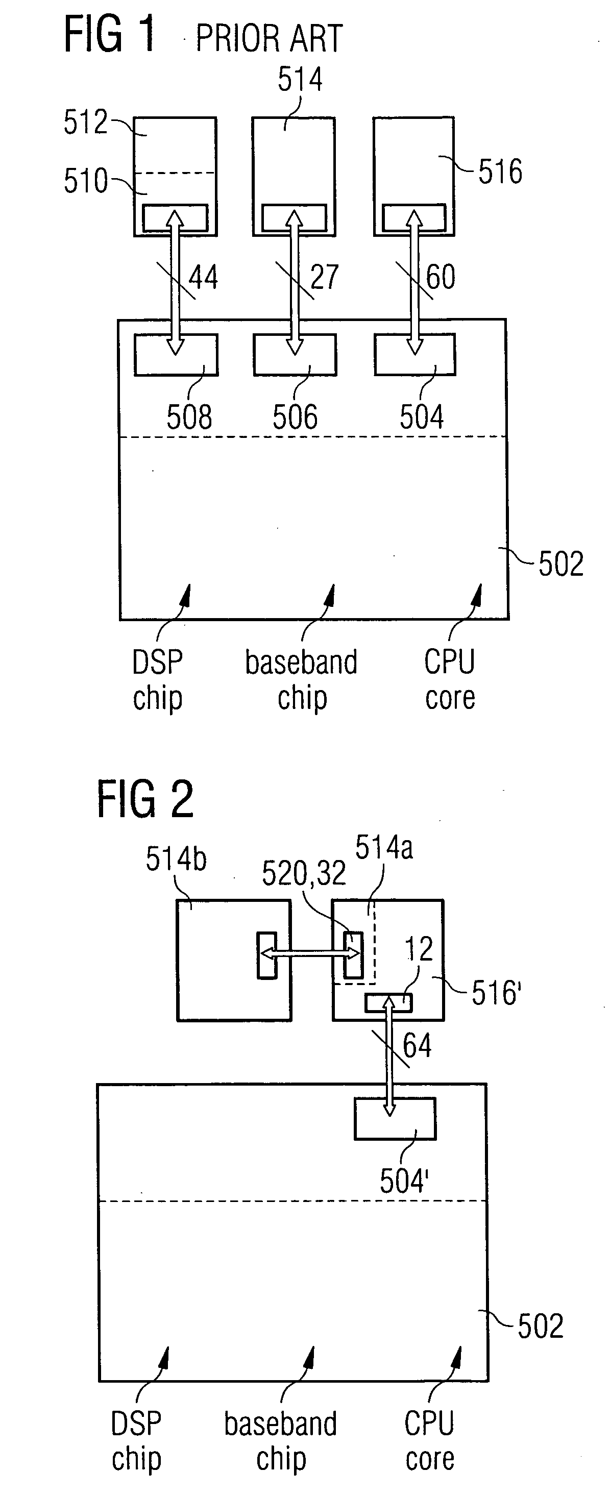
[0078]FIG. 2 shows an overview block diagram of a system comprising a CPU 502, an SDRAM work memory 516′ and a NAND-flash memory 514b for permanent storage of user data and executable program files according to the invention. CPU 502 has a single (first) interface 504′ that provides communication with both the volatile work memory 516′ and the non-volatile storage memory 514b. The width of this bus is increased to 64 data, command and address lines, or pins on the corresponding memory chip device, as compared with the 60 lines or pins shown in the prior art example of FIG. 1.

[0079] However, as interface 504′ is the only interface left on the CPU side, the total number of lines, or pads required on the CPU board 502, is reduced from 131 to 64 according to this specific example. Therein, the flash memory 514b is accessed via a second interface 520 from the SDRAM work memory 516′. More precisely, the SDRAM work memory 516′ comprises a NAND-flash controller section 514a, which controls ...

second embodiment

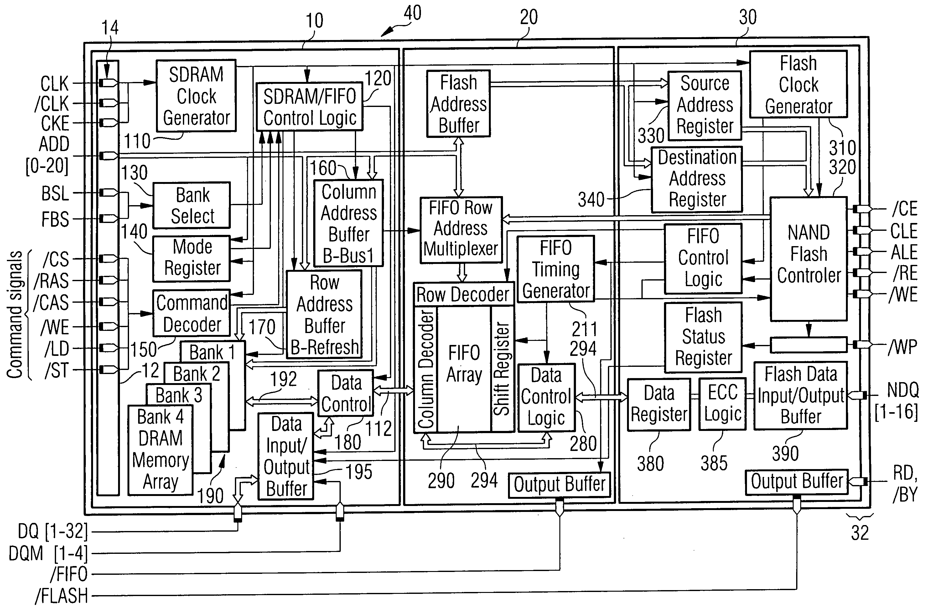
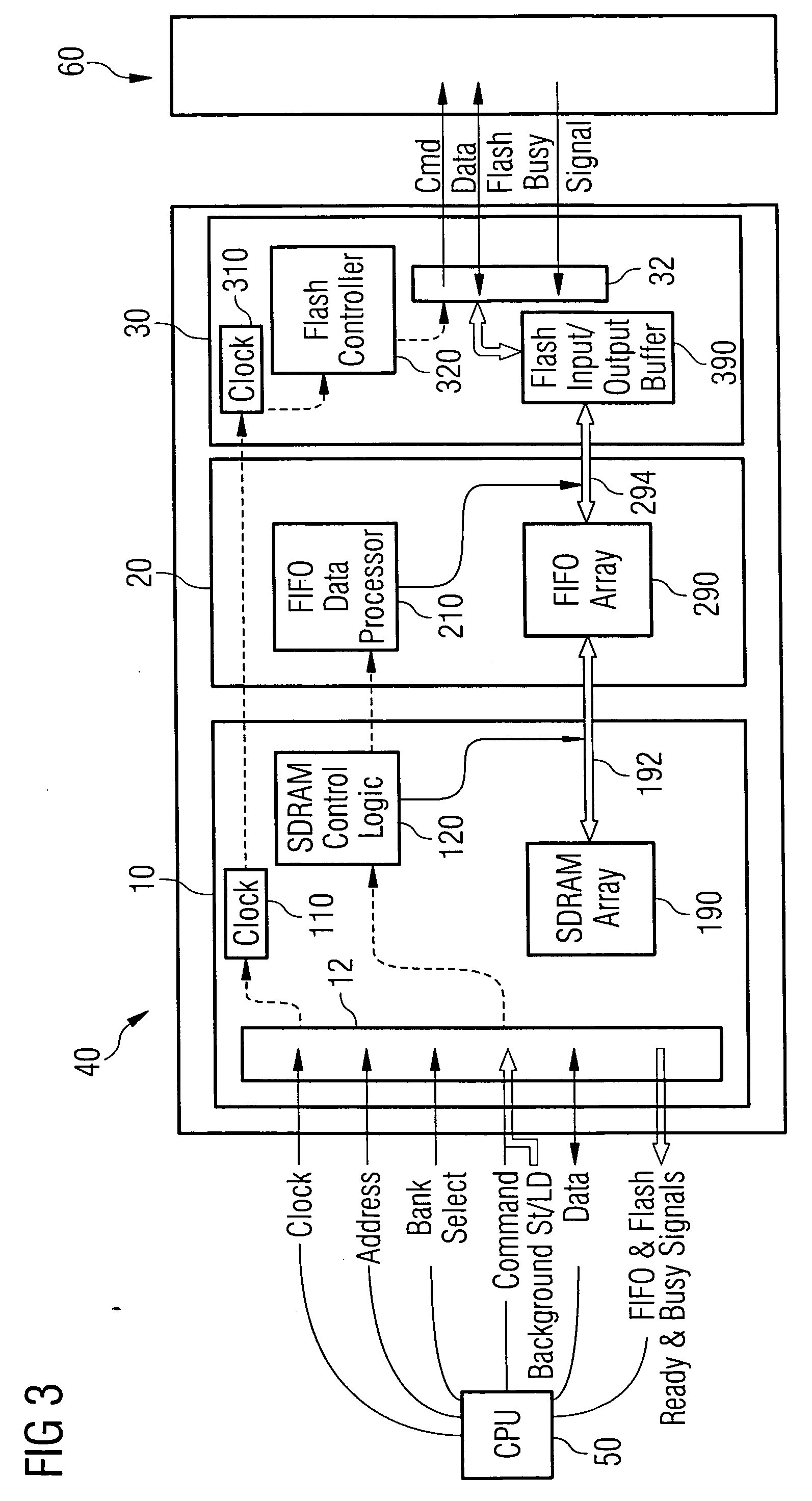
[0080]FIG. 3 shows a schematical block diagram with a similar SDRAM memory chip device 40, which is interfaced with a flash memory device 60 according to the present invention. The flash memory device 60 used in this embodiment is a NAND-flash memory.

[0081] The SDRAM memory chip device 40 according to this embodiment may be divided into three sections: an SDRAM core section 10, a FIFO buffer section 20 and a flash controller section 30. Nevertheless, all three sections may be manufactured on the same chip or die, while the flash memory device 60 accessed via the interface directly from the SDRAM memory device may be manufactured on another chip, or die.

[0082] The SDRAM core section 10 comprises an interface 12 to a host system such as a central processing unit 50 (CPU). The interface 12 comprises a plurality of pins 14, which are arranged to adhere to the SDRAM standard. According to their functions, the pins may be grouped into those transferring clock signals, address signals, co...


PUM


Abstract

An SDRAM memory chip device comprises a non-volatile memory controller for operating a non-volatile memory, e.g., a NAND-flash, and a FIFO memory buffer. The FIFO memory buffer serves to operate background store and load operations between a FIFO buffer array and the non-volatile memory, while a host system such as a CPU exchanges data with the SDRAM work memory. The SDRAM memory chip device, therefore, has at least two additional pins as compared with conventional SDRAM standard for generating a set of additional commands. These commands are employed by the FIFO memory buffer to manage the data transfer between the FIFO buffer and each of the non-volatile memory and the volatile SDRAM memory. Two further pins reflecting the flash memory status provide appropriate issuance of load or store signals by the host system.

Description

TECHNICAL FIELD [0001] The present invention relates generally to semiconductor components and, in various aspects, to a DRAM chip device well-communicated with flash memory chips and multi-chip packages comprising such a device. BACKGROUND [0002] Mobile systems such as cellular phones and digital cameras. have recently seen considerable improvements with respect to its system logic as well as its associated memory. According to the specific requirements of such a system, a variety of memory types is nowadays included into mobile systems simultaneously. [0003] For example, cellular phones as well as digital cameras have a system logic, which comprises a number of chips performing specific tasks associated with a mobile system. A cellular phone, e.g., has a base band chip for performing wireless communication tasks and further a digital signal processing (DSP) chip, which may control a charged coupled device (CCD) that is attached to a camera part of the cellular phone. [0004] Recent...

Claims


Application Information

Patent Timeline
IPC IPC(8): G06F12/00
CPCG06F13/1673G11C11/4093G11C7/10
Inventor FUKUZO, YUKIO
Owner INFINEON TECH AG
Why Eureka
Try Eureka