Thermal infrared image detector

a detector and infrared technology, applied in the direction of material analysis, optical radiation measurement, instruments, etc., can solve the problems of high temperature and high vacuum, increase the cost of array production, and difficult formation of ceramic materials in thin layers, etc., and achieve the effect of low cos

Inactive Publication Date: 2007-01-04
HAYES ROBERT STEPHEN
View PDF6 Cites 13 Cited by
  • Summary
  • Abstract
  • Description
  • Claims
  • Application Information

AI Technical Summary

Benefits of technology

[0005] It is an object of the invention to provide an infrared imaging device that can be fabricated using low cost materials that are not suitable for high tem

Problems solved by technology

These processes require high temperatures and high vacuum, which increases the cost of producing the array.
The ceramic material is difficult to form in thin layers.
This results in thermal conduction between detector elements which degrades the spatial resolution of the array.
The ceramic material also conducts heat to the substrate, which reduces the sensitivity of the array.
This is a slow and expensive process.
The sep

Method used


Image

  • Thermal infrared image detector
  • Thermal infrared image detector
  • Thermal infrared image detector

Examples


embodiment

Preferred Embodiment

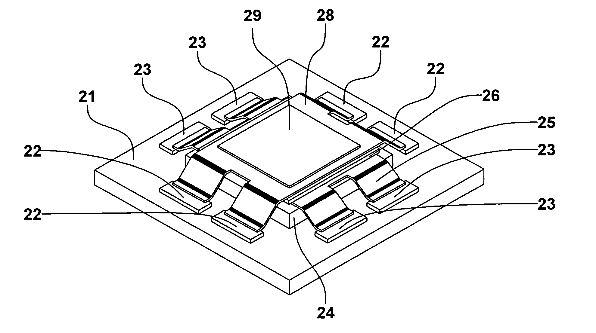
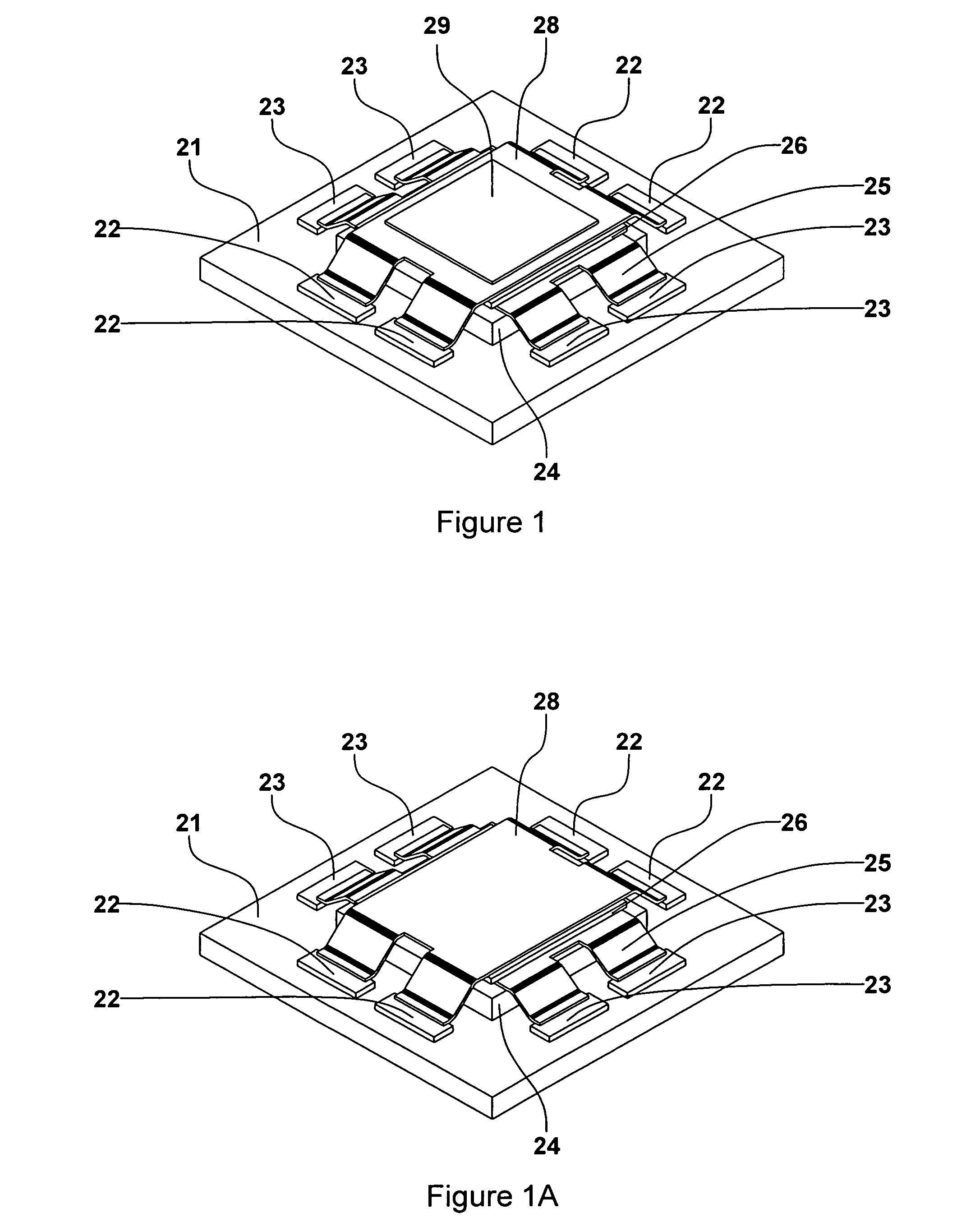
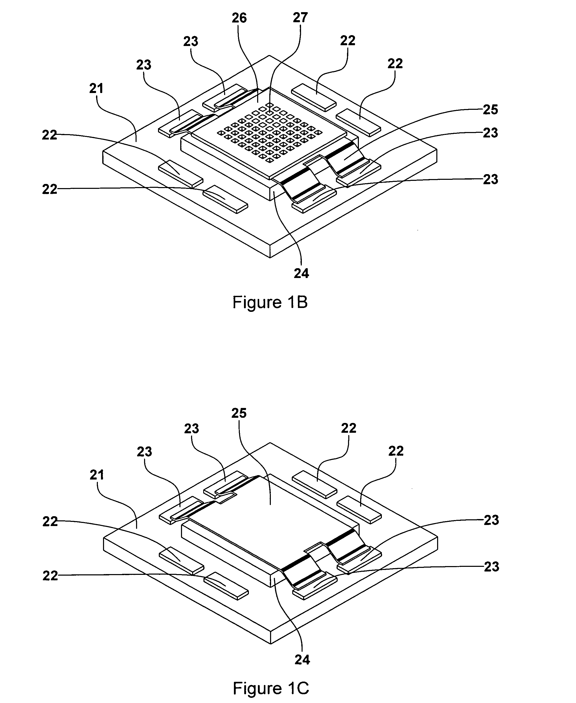
[0067]FIGS. 1 through 1F show a preferred embodiment of the detector assembly based on the use of a liquid crystal material as the thermally sensitive material.

[0068] The complete assembly is shown in FIG. 1. A substrate 21 supports the other parts of the assembly. The substrate temperature is controlled by a temperature control system and maintained at a temperature where the detector is most sensitive. The temperature of the substrate should be uniform in the area under the detector array. This may be achieved by using a thermally conductive material for the substrate, such as copper or kovar, or by making the substrate thick enough to allow lateral heat conduction. In this case, the substrate can be glass or ceramic.

[0069] Integrated circuits are mounted on the substrate to act as row drivers 22 and column amplifiers 23.

[0070] A thermal insulator 24 is mounted on the substrate. This insulator should be a material with high thermal resistance and low heat ca...

second embodiment

[0083] It is not essential that the row drivers 22 and column amplifiers 23 be incorporated into the detector assembly. FIG. 2 shows a detector assembly consisting of a lower electrode support 25 (with column electrodes), a spacer 26, liquid crystal material, an upper electrode support 28 (with row electrodes), and an infrared absorbing layer 29 mounted in a pin grid array package 33. The package would normally be closed with a window made of infrared transmissive material such as silicon. In this case, the row drivers and column amplifiers are not part of the detector assembly and can be constructed with either integrated circuits or discrete components in a separate assembly.

third embodiment

[0084] The row and column electrodes do not have to be on separate supports. FIGS. 3 (top view) and 3A (bottom view) show both sets of electrodes fabricated on a single support 34. This arrangement places the electrodes on the top side of the support with the row electrodes 31 surrounding the column electrodes 32. The gap between the electrodes has an electrostatic field that extends above the surface of the support for a small distance, and a dielectric material in this area will alter the capacitance between the electrodes depending on its dielectric constant. This electrode structure is useful where the dielectric material is incorporated in a paint, such as the commercially available liquid crystal paints, or is incorporated as a powder in a binder such as gelatin. If these electrodes are placed against the surface of a material whose dielectric constant varies with temperature, local changes in temperature will result in changes in capacitance which can be measured in the same ...


PUM


Abstract

The invention is a device for detecting images formed by thermal infrared radiation. It uses a two dimensional array of thermally sensitive elements formed of material whose capacitance changes with temperature. Changes in capacitance of the detector elements are measured and used to form an electronic representation of the thermal infared image. The detector array can be fabricated using inexpensive materials and processes.

Description

DESCRIPTION OF THE PRIOR ART [0001] Previous infrared image detectors, such as that disclosed by Hooper, in U.S. Pat. No. 4,080,532, have used pyroelectric ceramic materials operated at a temperature close to the Curie point of the ceramic material. The ceramic material is formed by sintering a mixture of materials at high temperature and then adding electrodes by vacuum deposition. These processes require high temperatures and high vacuum, which increases the cost of producing the array. The ceramic material is difficult to form in thin layers. This results in thermal conduction between detector elements which degrades the spatial resolution of the array. The ceramic material also conducts heat to the substrate, which reduces the sensitivity of the array. [0002] Another previous method of producing detector arrays is to use the techniques developed for integrated circuit production to form detectors by successive deposition and etching of several layers of different materials. The ...

Claims


Application Information

Patent Timeline
IPC IPC(8): G01J5/00
CPCG01J5/10G01J2005/345G01J2005/0077G01J5/34
Inventor HAYES, ROBERT STEPHEN
Owner HAYES ROBERT STEPHEN
Why Eureka
Try Eureka