
Superjunction semiconductor device

a superjunction semiconductor and semiconductor technology, applied in semiconductor devices, semiconductor/solid-state device details, electrical devices, etc., can solve the problems of reducing conductivity and switching speed, deteriorating the breakdown characteristics of superjunction semiconductor devices, and degrading the operating characteristic of devices, so as to prevent the breakdown characteristic from being deteriorated

Active Publication Date: 2007-01-04
SEMICON COMPONENTS IND LLC
View PDF6 Cites 83 Cited by
  • Summary
  • Abstract
  • Description
  • Claims
  • Application Information

AI Technical Summary

Benefits of technology

[0010] The present invention provides a superjunction semiconductor device for balancing the quantity of p charges and the quantity of n charges to prevent breakdown characteristic from being deteriorated in a specific region.
[0027] According to another aspect of the present invention, there is provided a superjunction semiconductor device including an edge p pillar and an active region. The edge p pillar has a rectangular ring shape with rounded corners. The active region is surrounded by the edge p pillar and has active p pillars and active n pillars having vertical stripe shapes. The active p pillars and the active n pillars are alternately arranged horizontally in the active region. Subsidiary p pillars are arranged in the active n pillars in the corners of the active region. The subsidiary p pillars compensate for an imbalance between the quantity of p charges and the quantity of n charges.

Problems solved by technology

This reduces conductivity and a switching speed, thereby degrading the operating characteristic of the device.
This deteriorates the breakdown characteristics of the superjunction semiconductor device.
These surplus p charges break the balance between the quantity of p charges and the quantity of n charges in the corners, upper and lower parts of the edge p pillar and result in a deterioration of the breakdown characteristics of the superjunction semiconductor device.

Method used


Image

  • Superjunction semiconductor device
  • Superjunction semiconductor device
  • Superjunction semiconductor device

Examples


first embodiment

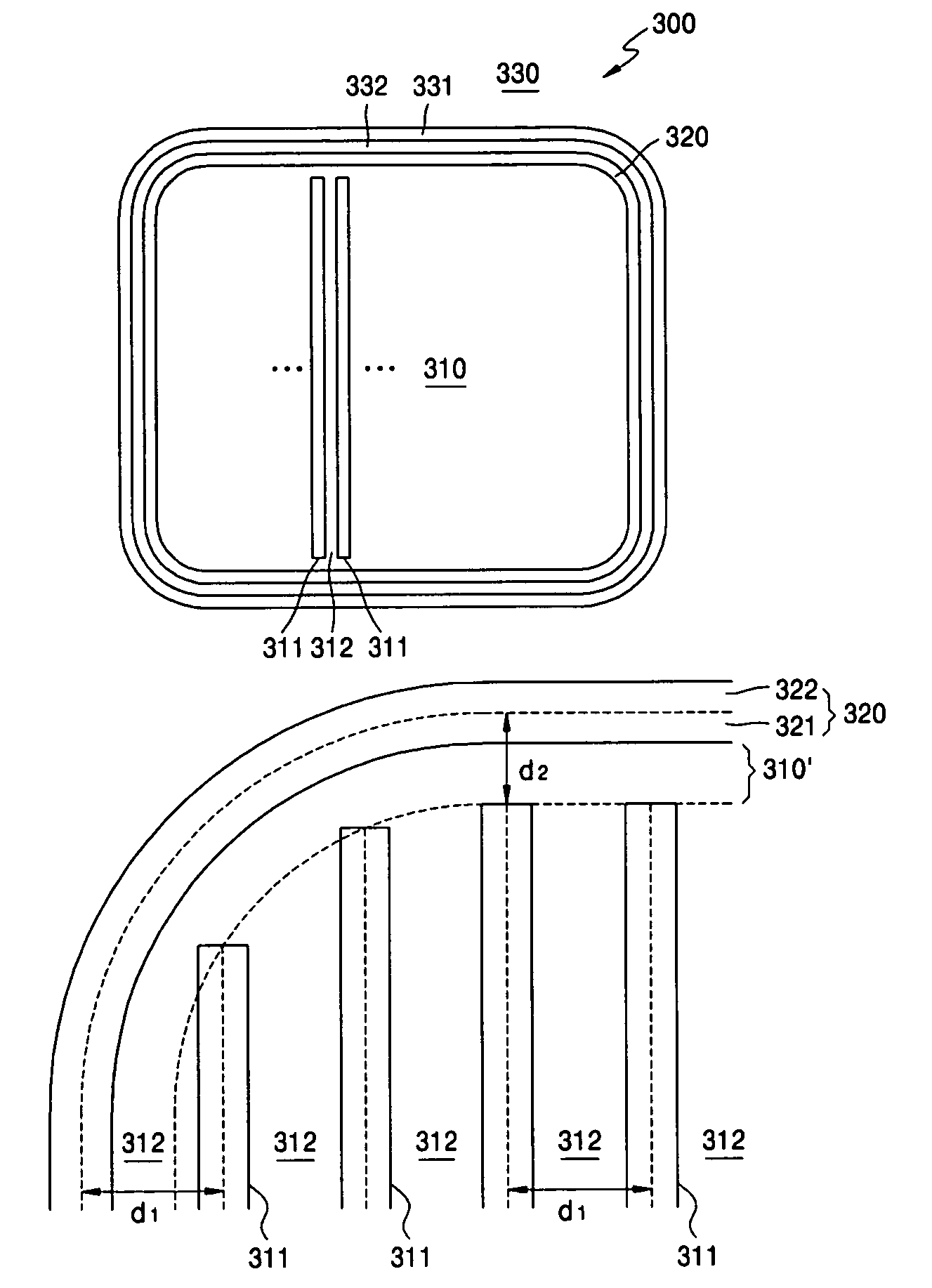
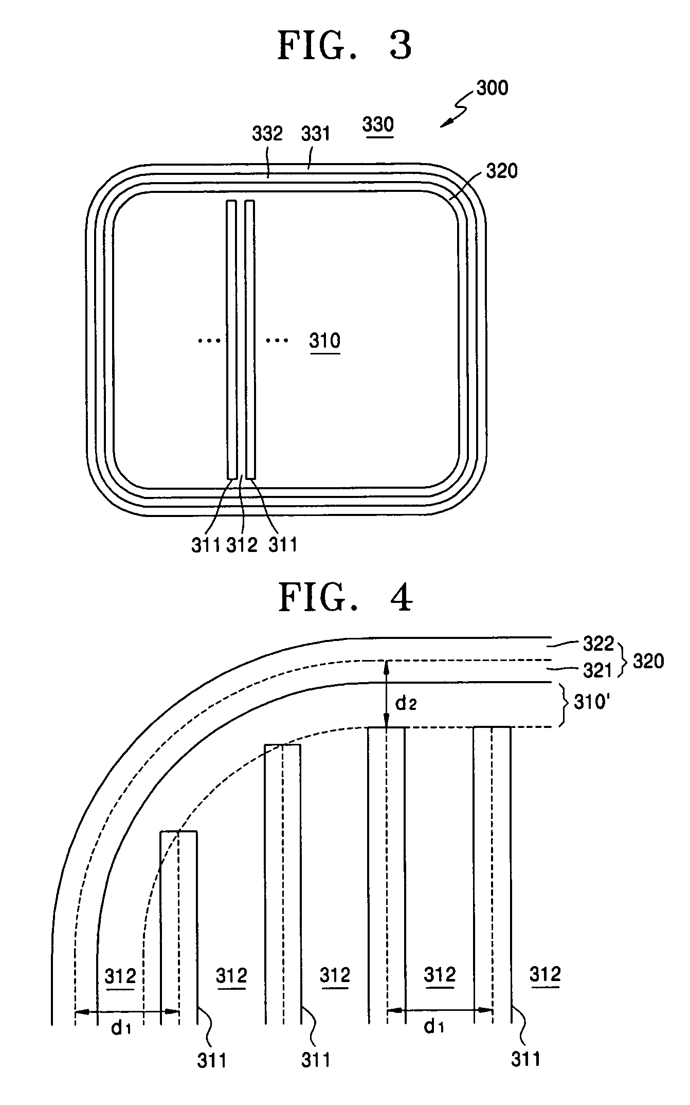
[0042]FIG. 3 is a layout of a superjunction semiconductor device 300 according to the present invention, and FIG. 4 illustrates a part of the superjunction semiconductor device 300, including a corner of the superjunction semiconductor device 300.

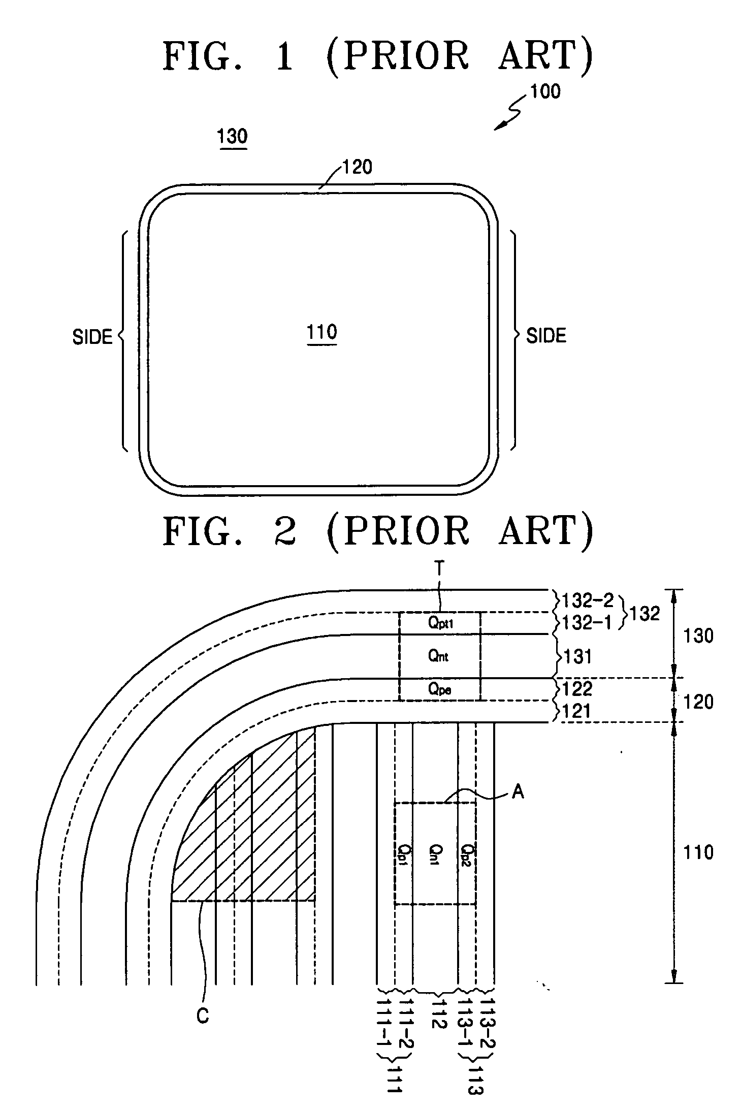
[0043] Referring to FIGS. 3 and 4, the superjunction semiconductor device 300 includes an active region 310 surrounded by an edge p pillar 320 in the form of a rectangular ring with rounded corners, and a termination region 330 surrounding the edge p pillar320. An active n region 312 is disposed in the active region 310, and active p pillars 311 having a striped pattern are arranged in the active n region 312 at predetermined intervals. The active n region 312 can be a conventional n type drift layer or a separate n type region formed on an n type drift layer, that is, an active n pillar. The top and bottom ends of the active p pillars 311 are separated from the edge p pillar 320. In the termination region 330, termination p pillars 331 and...

second embodiment

[0051]FIG. 9 is a layout of a superjunction semiconductor device 400 according to the present invention, and FIG. 10 illustrates a part of the superjunction semiconductor device 400, including a corner of the superjunction semiconductor device 400.

[0052] Referring to FIGS. 9 and 10, the superjunction semiconductor device 400 includes an active region 410 surrounded by an edge p pillar 420 having a first width W1 and rounded corners, and a termination region 430 surrounding the edge p pillar 420. The active region 410 has active p pillars 411 and active n pillars 412 having striped shapes which are alternately arranged horizontally. The termination region 430 includes termination p pillars 431 and termination n pillars 432 that have similar shape to the edge p pillar 420, and are alternately arranged. While the top and bottom ends of the active p pillars 311 of the active region 310 are separated from the edge p pillar 320 in the superjunction semiconductor device 300 according to th...

third embodiment

[0060]FIG. 15 is a layout of a superjunction semiconductor device 500 according to the present invention, and FIG. 16 illustrates a part of the superjunction semiconductor device 500, including a corner of the superjunction semiconductor device500.

[0061] Referring to FIGS. 15 and 16, the superjunction semiconductor device 500 includes an active region 510, an edge p pillar 520 having a rectangular ring shape with rounded corners and surrounding the active region 510, and a termination region 520 surrounding the edge p pillar 520. Active p pillars 511 and active n pillars 512 having striped shapes are alternately arranged in the horizontal direction in the active region 510. In the termination region 530, termination p pillars and termination n pillars (not shown) which have the same shape as the edge p pillar 520 are alternately arranged.

[0062] The edge p pillar 520 includes an inner region 521 adjacent to the active region 510 and an outer region 522 adjacent to the termination re...


PUM


Abstract

A superjunction semiconductor device includes an edge p pillar, an active region, and a termination region. The edge p pillar has a rectangular ring shape with rounded corners surrounding the active region. The active region includes an active n region and active p pillars having vertical stripe shapes disposed at regular intervals in the active n region. The top and bottom ends of the active p pillars are separated from the edge p pillar. The termination region includes termination n pillars and termination p pillars alternately arranged around the edge p pillar. Surplus p charges that are not used to balance the quantity of p charges and the quantity of n charges among p charges included in the upper and lower parts of the edge p pillar are eliminated or n charges are supplemented to balance the quantity of p charges and the quantity of n charges.

Description

CROSS-REFERENCES TO RELATED APPLICATIONS [0001] NOT APPLICABLE BACKGROUND OF THE INVENTION [0002] The present invention relates to a semiconductor device, and more particularly, to a superjunction semiconductor device having an alternating conductivity type drift layer. [0003] In general, a vertical type semiconductor device has a structure in which electrodes are arranged on two planes opposite to each other. When the vertical type semiconductor device is turned on, a drift current flows vertically in the semiconductor device. When the vertical type semiconductor device is turned off, depletion regions formed when a reverse bias voltage is applied to the device extend in the horizontal direction. To provide a high breakdown voltage to the vertical type semiconductor device, a drift layer disposed between the electrodes is formed of a material having high resistivity and the thickness of the drift layer is increased. In this case, however, an ON resistance of the device is also incr...

Claims


Application Information

Patent Timeline
IPC IPC(8): H01L29/76
CPCH01L29/0634
Inventor LEE, JAE-GILJUNG, JIN-YOUNGJANG, HO-CHEOL
Owner SEMICON COMPONENTS IND LLC
Features
  • Generate Ideas
  • Intellectual Property
  • Life Sciences
  • Materials
  • Tech Scout
  • Unparalleled Data Quality
  • Higher Quality Content
  • 60% Fewer Hallucinations
Learn More