

Driving circuit for switching elements
a technology of driving circuit and switching element, which is applied in the direction of electronic switching, electrical equipment, pulse technique, etc., can solve the problem of limit the capacity to prevent erroneous operation, and achieve the effect of improving the tolerance level of dv/dt transients and ensuring reliability
- Summary
- Abstract
- Description
- Claims
- Application Information
AI Technical Summary
Benefits of technology
Problems solved by technology
Method used
Image

Examples
embodiment 1
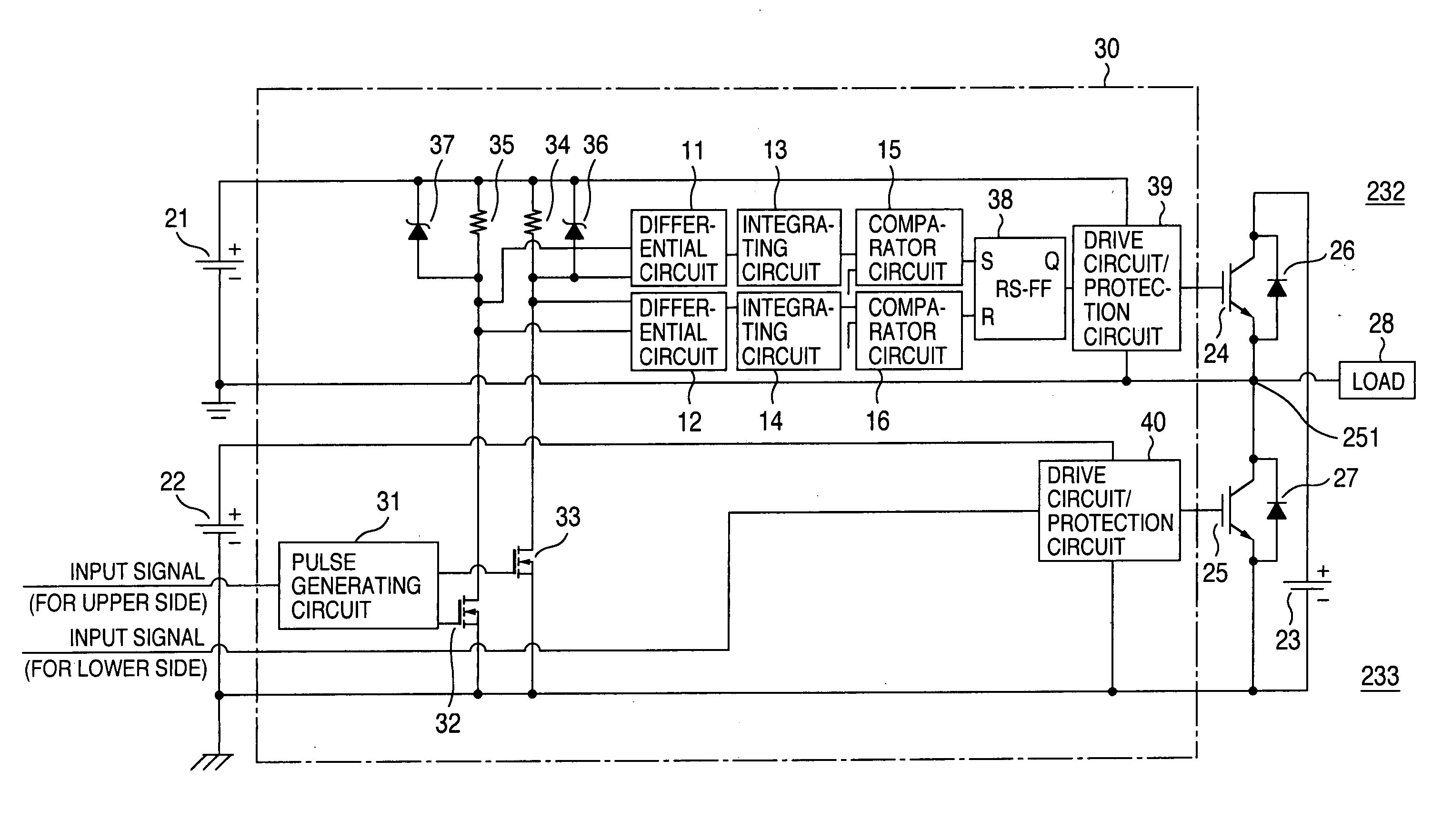
[0033]FIG. 1 is a block diagram showing the drive circuit of driver IC 30, a semiconductor device for driving a semiconductor power switching device being the embodiment. An IGBT (Insulated Gate Bipolar Transistor) 24, being the semiconductor power switching device (hereinafter abbreviated as “switching device”) of an upper side 232, and an IGBT 25, being the switching device of a lower side 233, are connected in totem-pole to both terminals of a main power supply 23 and constitute a half bridge. The cathode side of main power supply 23 is connected to ground.
[0034] Freewheel diodes 26, 27 are connected in anti-parallel to IGBT 24 and IGBT 25. And, a load 28 (an inductive load like a motor) is connected to a connection point 251 of IGBT 24 and IGBT 25.
[0035] IGBT 24 of upper side 232 is a device performing switching operation, taking as reference potential the potential of the point 251 of contact with IGBT 25 of lower side 233, and an upper side regulating power supply 21 insulat...
embodiment 2
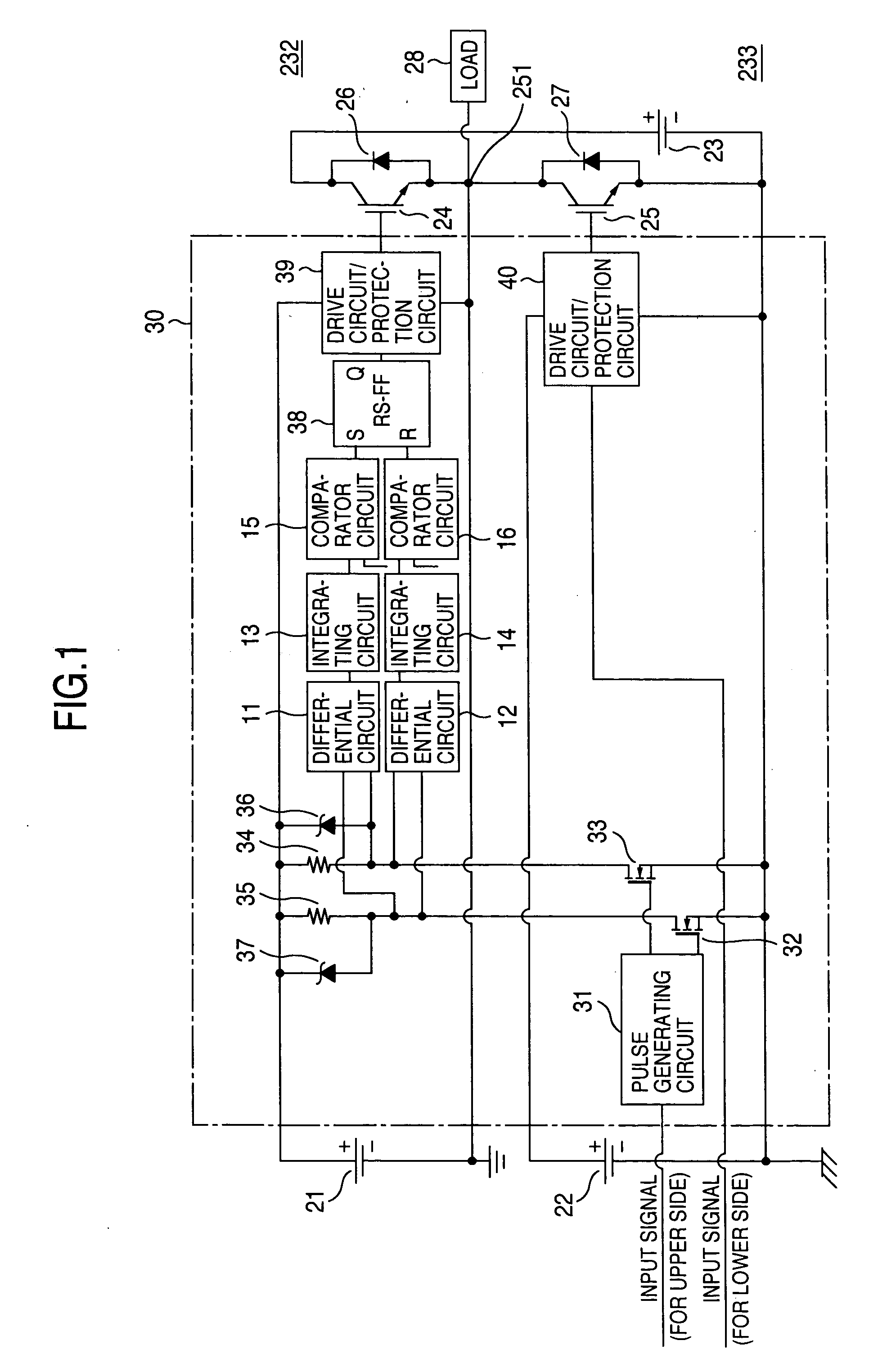
[0051]FIG. 3 is block diagram showing the present embodiment 2. To constituent elements identical to those of FIG. 1, identical symbols are attached. The present embodiment has the configuration of Embodiment 1, but with integrating circuits 13, 14 removed.
[0052] The differential voltage, during normal operation, is outputted with a value corresponding to the pulse width. Because of this, it is determined to be at a regular level and is outputted as a normal signal, and is inputted as a signal to the set input and the reset input of flip-flop circuit 38.
[0053] Moreover, in case a dV / dt transient signal is generated, since the difference of the simultaneously flowing currents is obtained in set differential amplifier circuit 11 and reset differential amplifier circuit 12, the outputs of the differential amplifier circuits almost reach zero. Consequently, in these circuits, since differential voltages are obtained, the outputs of the differential amplifier circuits almost reach zero...
embodiment 3
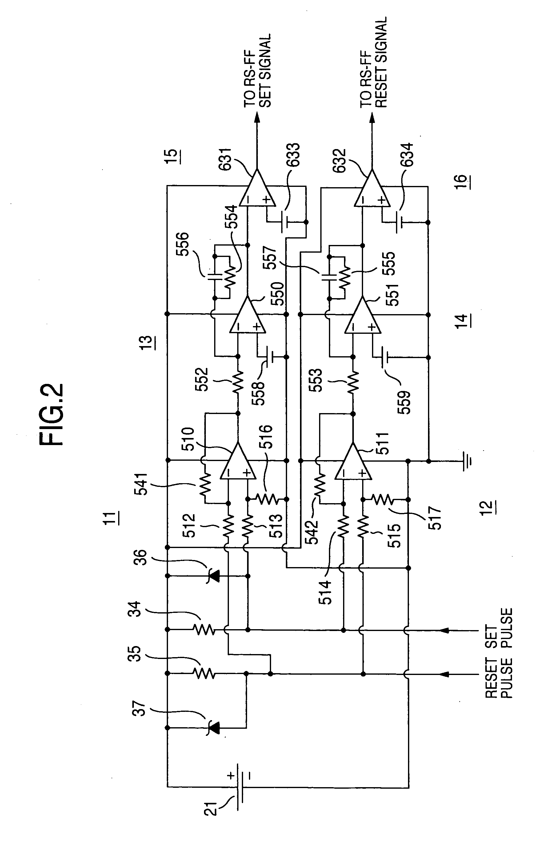
[0055]FIG. 5 is a block diagram showing the circuits of the present embodiment. Elements identical to those in Embodiment 1 have the same symbols attached. The present embodiment has the configuration of Embodiment 2, but with differential amplifier circuits 11, 12 removed, and the voltages of level shifting resistances 34, 35 are supplied directly to comparator circuits 15, 16.
[0056] With comparator circuits 15, 16, it is possible to set a low level for the variation in reference potential, and, by taking advantage of the delay time of comparator circuits 15, 16, the integrated value of the regular signal and the integrated value of the dV / dt noise signal are calculated in advance. When the comparison voltages of comparator circuits 15, 16 are set appropriately, simultaneous inputting of signals in the set input and the reset input of flip-flop circuit 38 is eliminated, even in the present configuration. Because of this, it becomes possible to prevent generating unpredictable oper...
PUM
 Abstract
Description
Claims
Application Information