Color filter substrate for organic EL element

a technology of electroluminescent elements and substrates, which is applied in the direction of luminescnet screens, natural mineral layered products, discharge tubes, etc., can solve the problems of inability to achieve the coating-solution based on inability to produce fine particles with the average particle size of too small, and inability to achieve the above-mentioned size effect at firing temperature , to achieve the effect of preventing the generation of defects such as dark spots

Inactive Publication Date: 2007-01-04
DAI NIPPON PRINTING CO LTD
View PDF1 Cites 47 Cited by
  • Summary
  • Abstract
  • Description
  • Claims
  • Application Information

AI Technical Summary

Benefits of technology

[0060] According to the invention, the generation of defects such as dark spots can be restrained to produce an organic EL display device capable of attaining good image display since the above-mentioned color filter substrate for an organic EL element is used. Moreover, it is unnecessary to form a thick transparent barrier layer as in the prior art. Thus, an inexpensive organic EL display device can be provided.
[0061] According to the invention, good barrier property can be obtained by laminating the transparent electrode layer and the conductive layer. Thus, when the color filter substrate for an organic EL element of the invention is used in an organic EL display device, the generation of dark spots can be restrained. Moreover, it is unnecessary to form a thick transparent barrier layer as in the prior art. Thus, an advantageous effect of making costs low is produced.
[0062] The formation of the transparent electrode layer on / over the conductive layer makes it possible to improve adhesive force between the transparent electrode layer and the colored layer, and restrain the generation of peeling or cracking in the interfaces between the substrate on / over which the colored layer is formed and the transparent electrode layer.

Problems solved by technology

Fine particles with the average particle size thereof too small are not easily produced.
On the other hand, if the average particle size of the fine particles is too large, pinholes or other detects in the transparent electrode layer may not be easily blocked.
Moreover, the fall in the firing temperature the coating-solution based on the above-mentioned size effect cannot be expected.

Method used


Image

  • Color filter substrate for organic EL element
  • Color filter substrate for organic EL element
  • Color filter substrate for organic EL element

Examples


first embodiment

1. First Embodiment

[0095] The first embodiment of the color filter substrate for an organic EL element of the invention is a color filter substrate for an organic EL element having a substrate, a colored layer formed in a pattern form on / over the substrate, a transparent electrode layer formed on / over the colored layer, and a conductive layer formed on / over the transparent electrode layer and having barrier property, wherein the conductive layer is a coated film.

[0096] The color filter substrate for an organic EL element of the embodiment will be explained with a reference to the drawings.

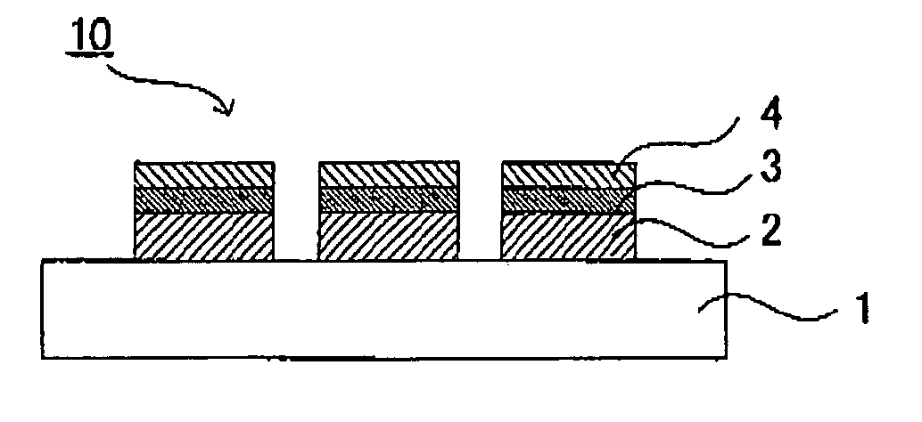
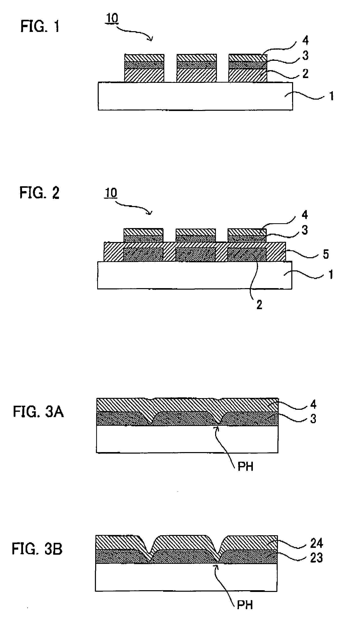
[0097]FIG. 1 is a schematic sectional view showing an example of the color filter substrate For an organic EL element of the present embodiment. As shown in FIG. 1, a color filter substrate for an organic EL element 10 according to this embodiment is a product in which a colored layer 2, a transparent electrode layer 3 and a conductive layer 4 are successively formed in a pattern form on a substr...

second embodiment

II. Second Embodiment

[0353] The following describes the second embodiment of the color filter substrate for an organic EL element of the present invention.

[0354] The second embodiment of the color filter substrate for an organic EL element of the present invention is characterized in providing a color filter substrate for organic EL element having a substrate, a colored layer formed in a pattern form on / over the substrate, a transparent electrode layer formed on / over the colored layer, and a conductive layer formed on / over the transparent electrode layer, wherein pinholes present in the transparent electrode layer are blocked with the conductive layer.

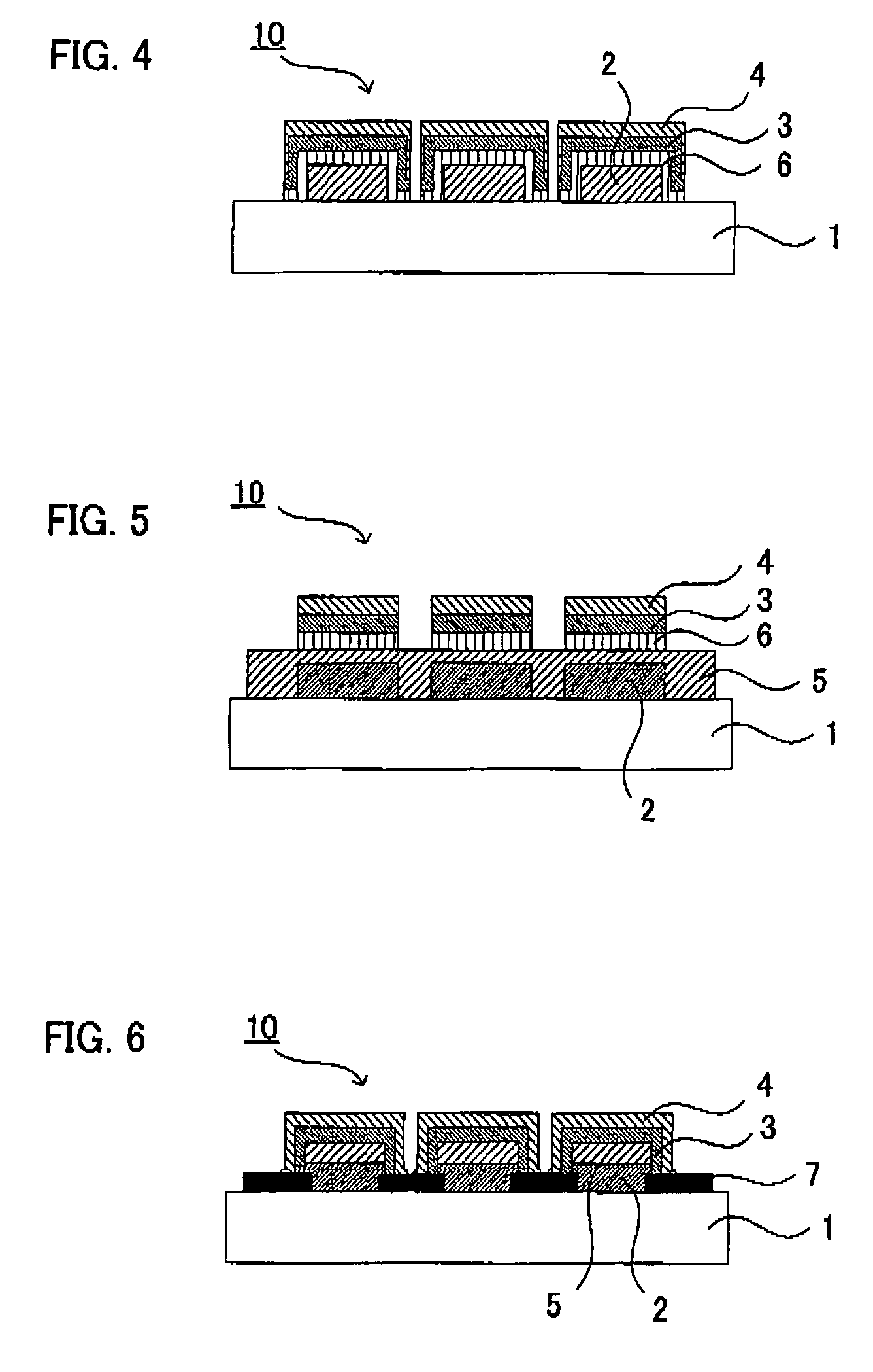
[0355] It is allowable in the embodiment that an overcoat layer 5 is formed between the colored layer 2 and the transparent electrode layer 3 as shown in FIG. 2.

[0356] As shown in, e.g., FIG. 3A, in the embodiment, pinholes PH present in the transparent electrode layer 3 are blocked with the conductive layer 4; therefore, barrier pr...

example 1

(Formation of a Black Matrix)

[0391] As a transparent substrate, prepared was a 370 mm×470 mm×0.7 mm (thickness) sodium glass substrate (a Sn face polished product, manufactured by CENTRAL GLASS CO., LTD). This transparent substrate was washed by an ordinary method, and then a thin film (thickness: 0.2 μm) made of chromium nitride oxide complex was formed on the whole of one surface of the transparent substrate. A photosensitive resist was coated onto this thin film, and the resultant was subjected to mask-exposure and development. The thin film was then etched, thereby yielding a black matrix in which openings each having a 84 μm×284 μm rectangular shape were arranged at a pitch of 100 μm in a matrix form.

(Formation of a Colored Layer)

[0392] Prepared were photosensitive coating compositions for forming colored layers in three colors of red, green and blue. As a red coloring agent, a green coloring agent and a blue coloring agent, the following were used: a condensed azo dye (Ch...


PUM

PropertyMeasurementUnit
particle sizeaaaaaaaaaa
voltageaaaaaaaaaa
thicknessaaaaaaaaaa

Abstract

The main object of the present invention is to provide an inexpensive color filter substrate for an organic EL element and an organic EL display device which are capable of displaying good images having no defects such as dark spots. To attain the object, the invention provides a color filter substrate for an organic EL element having a substrate, a colored layer formed in a pattern form on/over the substrate, and a transparent electrode layer and a conductive layer laminated, in any order, on/over the colored layer, wherein the conductive layer is a coated film.

Description

BACKGROUND OF THE INVENTION [0001] 1. Field of the Invention [0002] The present invention relates to a color filter substrate for an organic electroluminescent element, which is used in an organic electroluminescent display device capable of attaining color display. [0003] 2. Description of the Related Art [0004] Organic electroluminescent (hereinafter, may refer to as organic EL) elements have high luminous efficiency. Thus, for example, the elements realize highly bright luminescence even if the voltage applied thereto is a little less than 10V. Moreover, from a simple structure thereof, light can be emitted. Therefore, the application thereof to image display devices has been expected and research thereon has been actively made. In particular, an organic EL element has been increasingly made practicable as a luminescent element in an image display device since the organic EL element has the following advantages; the element has high visibility by its self color-development; the e...

Claims


Application Information

Patent Timeline
Patent Type & Authority Applications(United States)
IPC IPC(8): B32B3/10H01L51/52H05B33/02
CPCB82Y20/00B82Y30/00H01L27/322H01L51/5206Y10T428/24851H01L2251/5369H05B33/28Y10T428/256Y10T428/25H01L51/5237H10K59/38H10K50/816H10K50/844H10K2102/331H10K71/861H05B33/04
Inventor ASANO, MASAAKIBABA, YASUKOOSHIGE, HIDEMASAMIYOSHI, TATSUYA
Owner DAI NIPPON PRINTING CO LTD
Why Eureka
Try Eureka