Semiconductor integrated circuit, standard cell, standard cell library, semiconductor integrated circuit designing method, and semiconductor integrated circuit designing equipment

a technology of semiconductor integrated circuit and design method, which is applied in the direction of instruments, originals for photomechanical treatment, optics, etc., can solve the problems of increased propagation delay time, delay in tat (turn around time), and increased processing amoun

Active Publication Date: 2007-01-04
PANASONIC CORP
View PDF11 Cites 82 Cited by
  • Summary
  • Abstract
  • Description
  • Claims
  • Application Information

AI Technical Summary

Benefits of technology

[0019] As described above, the present invention limits a neighboring gate pattern to be arranged adjacent to a gate pattern including the transistor to be active as a correction target in OPC p

Problems solved by technology

For this reason, the dispersion of propagation delay time increases, which in turn requires a large design margin to make it difficult to provide a high performance semiconductor integrated circuit.
However, the gate mask correction through OPC invites delay in TAT (Turn Around Time) and an increase in processing amount.
However, this lowers outstandingly the flexibility of design, inviting degr

Method used


Image

  • Semiconductor integrated circuit, standard cell, standard cell library, semiconductor integrated circuit designing method, and semiconductor integrated circuit designing equipment
  • Semiconductor integrated circuit, standard cell, standard cell library, semiconductor integrated circuit designing method, and semiconductor integrated circuit designing equipment
  • Semiconductor integrated circuit, standard cell, standard cell library, semiconductor integrated circuit designing method, and semiconductor integrated circuit designing equipment

Examples


embodiment 1

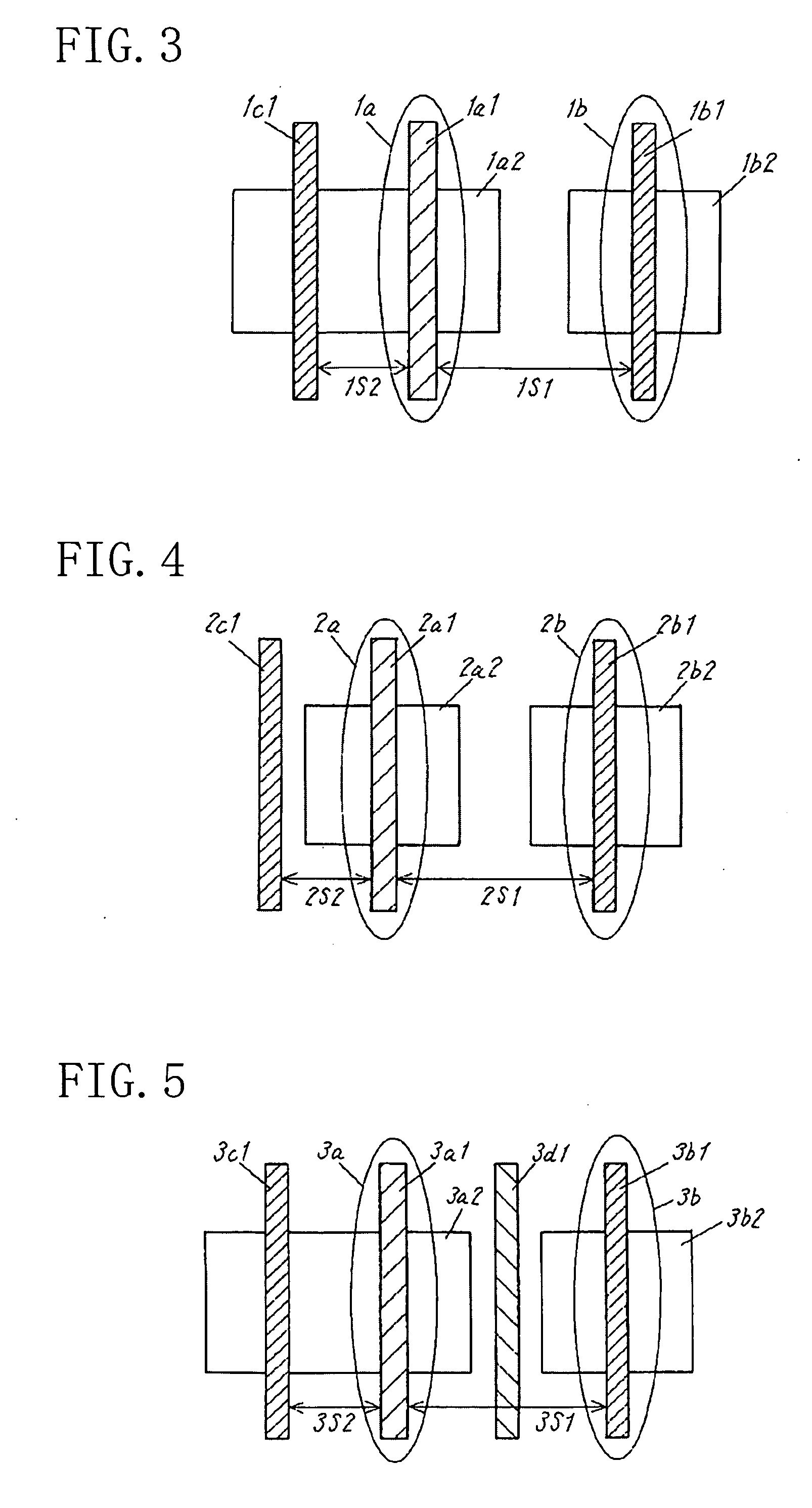
[0059]FIG. 3 is a layout diagram showing a layout pattern of a semiconductor integrated circuit according to Embodiment 1 of the present invention. In FIG. 3, a transistor 1b and a gate 1c1 are arranged on the respective sides of an active transistor 1a. The active transistor 1a is formed of a gate 1a1 and a diffusion region 1a2 while the transistor 1b is formed of a gate 1b1 and a diffusion region 1b2. The transistor 1b and the gate 1c1 are arranged adjacent to the active transistor 1a in a direction intersected at a right angle with a direction that the gate 1a1 extends.

[0060] The gate 1a1, the gate 1b1, and the gate 1c1 are arranged so that a space 1S1 between the gate 1a1 and the gate 1b1 is larger than a space 1S2 between the gate 1a1 and the gate 1c1 (for example, the space 1S1 is set so as to be two times, preferably, three times or more the space 1S2). The arrangement in which the space between the gate 1a1 and the gate 1b1 is set wide reduces the optical proximity effect t...

embodiment 2

[0061]FIG. 4 is a layout diagram showing a layout pattern of a semiconductor integrated circuit according to Embodiment 2 of the present invention. In FIG. 4, an active transistor 2a is formed of a gate 2a1 and a diffusion region 2a2 while a transistor 2b is formed of a gate 2b1 and a diffusion region 2b2.

[0062] Difference of FIG. 4 from FIG. 3 lies in that a dummy gate 2c1 is provided in lieu to the gate 1c1. Even with the dummy gate 2c1, the arrangement in which the space between the gate 2a1 and the gate 2b1 is set wide attains the same effects as those in Embodiment 1.

embodiment 3

[0063]FIG. 5 is a layout diagram showing a layout pattern of a semiconductor integrated circuit according to Embodiment 3 of the present invention. In FIG. 5, an active transistor 3a is formed of a gate 3a1 and a diffusion region 3a2 while a transistor 3b is formed of a gate 3b1 and a diffusion region 3b2.

[0064] Difference of FIG. 5 from FIG. 3 lies in that a dummy gate 3d1 is arranged in parallel to the gate 3a1 between the gate 3a1 of the active transistor 3a and the gate 3b1 of the transistor 3b. When the additional gate 3d1 is interposed between the gate 3a1 of the active transistor 3a and the gate 3b1 of the transistor 3b, as shown in FIG. 5, influence of dimensional dispersion by the optical proximity that the gate 3b1 of the transistor 3b gives to the gate 3a1 of the active transistor 3a can be suppressed further than that in Embodiment 1.


PUM


Abstract

A semiconductor integrated circuit includes a first transistor which is formed of a first gate extending in a first direction and a first diffusion region and which is capable of being active, a second transistor which is formed of a second gate extending in the first direction and a second diffusion region and which is arranged adjacent to the first transistor in a second direction intersected at a right angle with the first direction, and a third gate which extends in the first direction and which is arranged adjacent in the second direction to the first transistor on an opposite side to the second transistor. A space between the first gate and the second gate is larger than a space between the first gate and the third gate.

Description

CROSS REFERENCE TO RELATED APPLICATIONS [0001] This Non-provisional application claims priority under 35 U.S.C. § 119(a) on Patent Application No. 2005-191433 filed in Japan on Jun. 30, 2005, the entire contents of which are hereby incorporated by reference. BACKGROUND OF THE INVENTION [0002] The present invention relates to a semiconductor integrated circuit and a designing technique thereof and particularly relates to an effective technique for suppressing optical proximity effect. [0003] In a semiconductor integrated circuit, main factors of dispersion of propagation delay time of signals are dispersion of power supply voltage in operation, dispersion of temperature, dispersion in the manufacturing process, and the like. The semiconductor integrated circuits must be designed so that the operation thereof is guaranteed even when all the above factors of dispersion become the worst. Particularly, gate length of a transistor plays a significant role for defining the operation of the...

Claims


Application Information

Patent Timeline
IPC IPC(8): H01L27/10H01L21/336G03F1/36G03F1/68G03F1/70H01L21/027H01L21/82
CPCG06F17/5072H01L27/11807H01L27/0207G06F30/392
Inventor TOUBOU, TETSUROUOKAMOTO, NANAYANO, JUNICHI
Owner PANASONIC CORP
Why Eureka
Try Eureka