Method for manufacturing a flexible panel for a flat panel display

Inactive Publication Date: 2007-01-04
IND TECH RES INST
6 Cites 8 Cited by

AI-Extracted Technical Summary

Problems solved by technology

However, the device characteristics and film quality made on the plastic substrate are inferior to those made on the glass substrate because the plastic substrate can not resist to the high-processing temperature, around 300 to 400 degrees C. Although Sharp Co. has developed a plastic substrate that is capable of withstanding up to approx. 220 degrees C., there is still a need to re-design or modify the conventional FPD process due to the plasticity and flexibility of the plastic substrate.
Besides, such technique is quite difficult and low yield rate.
As for organic ...

Method used

[0027] Example 3 of the present invention shows an even easier method for manufacturing a flexible panel. After the thin film devices are formed and the first substrate is thinned, the surface of the whole product is coated wi...

Benefits of technology

[0009] The object of the present invention is to provide a method for manufacturing a flexible panel so that the thin film devices formed on a glass subs...

Abstract

A method for manufacturing a flexible panel is disclosed, which has the following steps. First, a first substrate having a plurality of functional switches or conducting lines thereon is provided. Then, a second substrate is bonded on the functional switches or conducting lines, and the first substrate is thinned to a predetermined thickness subsequently. Afterwards, a flexible third substrate is adhered on the first substrate, wherein the first substrate is sandwiched between the second substrate and the third substrate. Finally, the second substrate is removed.

Application Domain

Gas-filled discharge tubesLamination ancillary operations +7

Technology Topic

Image

  • Method for manufacturing a flexible panel for a flat panel display
  • Method for manufacturing a flexible panel for a flat panel display
  • Method for manufacturing a flexible panel for a flat panel display

Examples

  • Experimental program(3)

Example

EXAMPLE 1
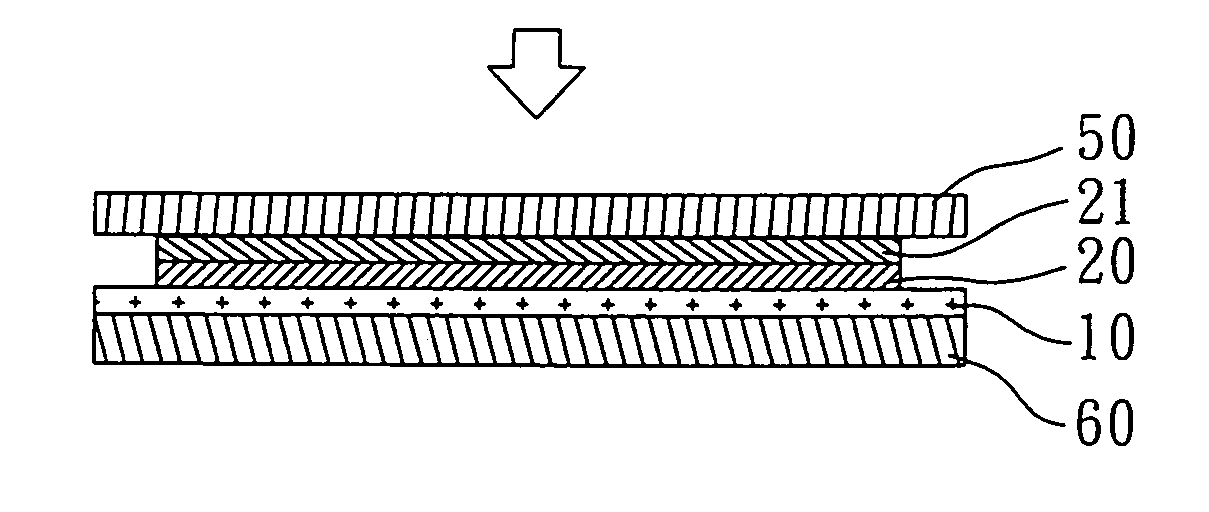
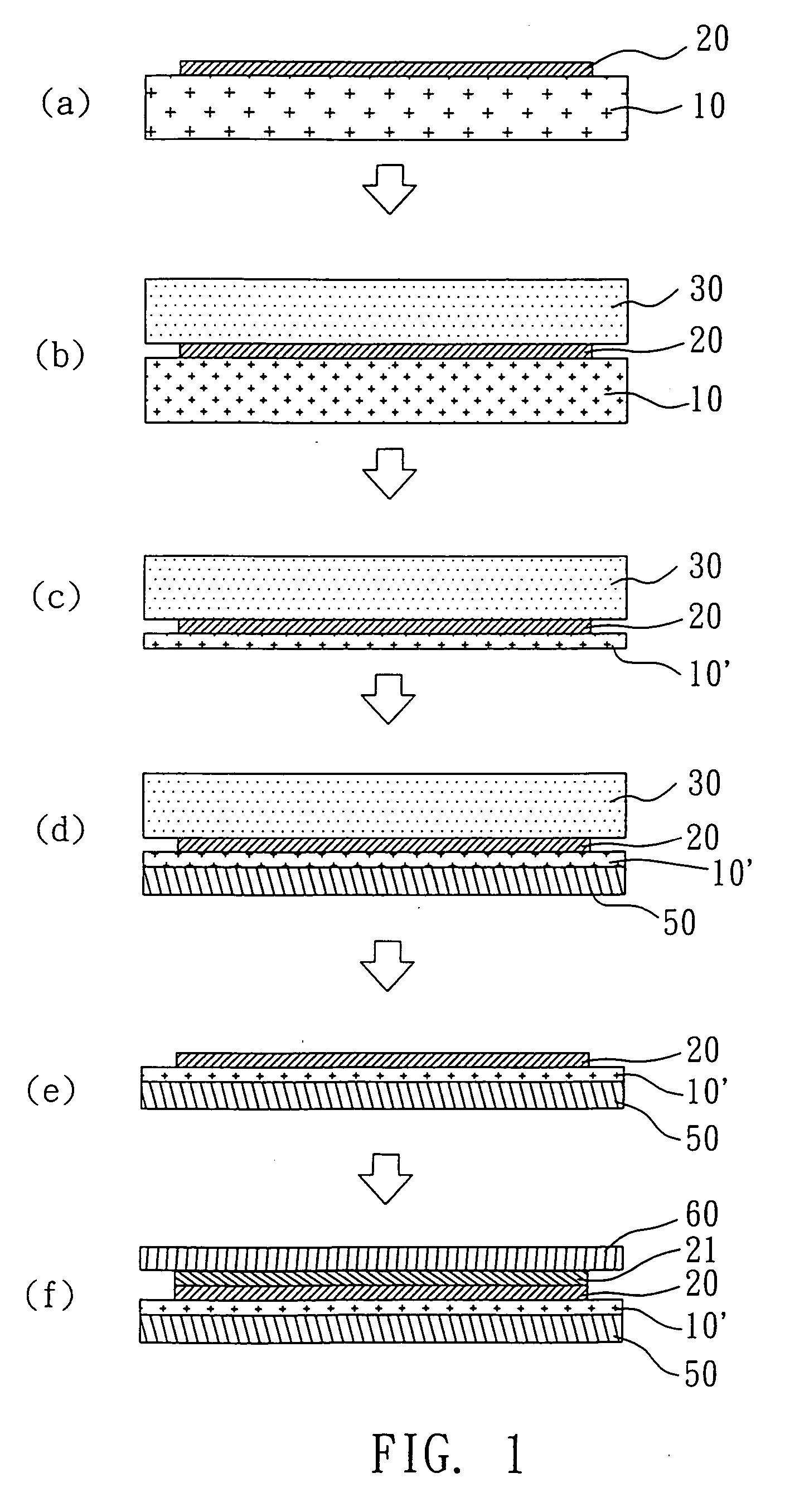
[0021] With reference to FIG. 1, there is shown the flow diagram of the first example of the present invention. The method for manufacturing a flexible panel of the present invention includes the following steps. First, a first substrate 10 is provided having a plurality of functional switches or conducting lines 20 formed thereon. The functional switches may be thin film transistors. Next, the second substrate 30 is bonded on the functional switches or conducting lines 20. Afterwards, the first substrate 10 is thinned to a predetermined thickness. The flexible third substrate 50 is subsequently adhered on the thinned first substrate 10′ so that the thinned first substrate 10′ is sandwiched between the second substrate 30 and the flexible third substrate 50. Finally, the second substrate 30 is removed.
[0022] It is optional to form a plurality of light valves, light-emitters, or conducting layers 21 on the functional switches or conducting lines 20 and then the flexible fourth substrate 60 is adhered on the light valves, light-emitters, or conducting layers 21 after the second substrate 30 is removed so that the light valves, light-emitters, or conducting layers 21 are located between the third substrate 50 and the fourth substrate 60. The light valve is a liquid crystal display device, and the light-emitter is an organic electroluminescent display device.

Example

Example 2
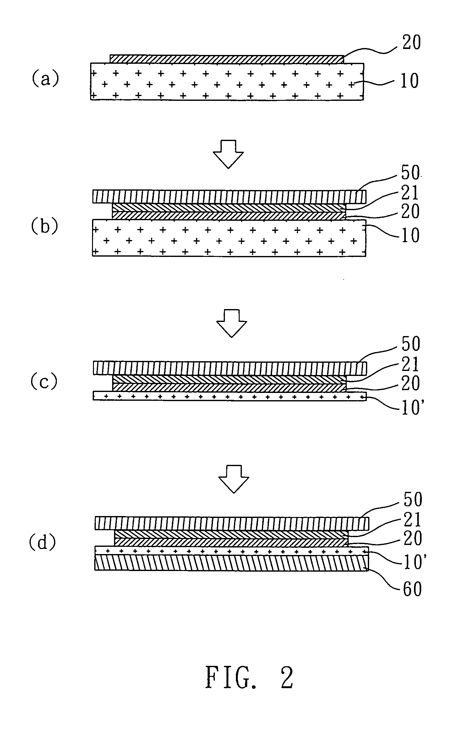
[0023] With reference to FIG. 2, there is shown the flow diagram of the second example of the present invention. The method for manufacturing a flexible panel of the present example will be illustrated as follows. The first substrate 10 having a plurality of functional switches or conducting lines 20 formed thereon is provided first. Afterwards, a plurality of light valves, light-emitters, or conducting layers 21 is formed on the functional switches or conducting lines 20, and the flexible third substrate 50 is adhered on the light valves, light-emitters, or conducting layers 21. As a result, the functional switches or conducting lines 20 and the light valves, light-emitters, or conducting layers 21 are sandwiched between the first substrate 10 and the third substrate 50. The first substrate 10 is then thinned to a predetermined thickness and forms the thinned first substrate 10′. Finally, the flexible fourth substrate 60 is adhered on the thinned first substrate 10′ so that the functional switches or conducting lines 20 and the light valves, light-emitters, or conducting layers 21 are located between the third substrate 50 and the fourth substrate 60.

Example

Example 3
[0024] With reference to FIG. 3, there is shown the flow diagram of the third example of the present invention. The method for manufacturing a flexible panel of the present example will be illustrated as follows. The first substrate 10 having a plurality of functional switches or conducting lines 20 formed thereon is provided first. The functional switches are thin film transistors in the present example. Next, the second substrate 30 is bonded on the functional switches or conducting lines 20, and then the first substrate 10 is thinned to a predetermined thickness to form the thinned first substrate 10′. Afterwards, the fifth substrate 70 is adhered on the thinned first substrate 10′ and subsequently the second substrate 30 is removed. Next, a plurality of light valves, light-emitters, or conducting layers 21 is formed on the functional switches or conducting lines 20, and then the fifth substrate 70 is removed. Finally, the surface of the whole substrate is coated with a flexible polymer layer 40.
[0025] In the foresaid three examples, the functional switches can be any well-known switches for electricity. Preferably, the functional switch is a thin film transistor or a diode. The second substrate as described above works for supporting the first substrate during the thinning step and preventing the first substrate from breaking. The thinning method is optionally selected from polishing, cutting, and etching. Preferably, the first substrate is thinned to have a thickness ranging from 30 to 100 μm.
[0026] The third and fourth substrates aforementioned are made of flexible materials that are generally used, or polymers. Among them, the plastics have the most potential. The plastics are limited in conventional applications as they cannot endure the high temperature. Nevertheless, this problem has been overcome by the present invention. The present invention forms the thin film devices on the glass substrate, which is then thinned and bonded with the plastic substrate. While the plastic substrate does not have to proceed with a high temperature process, the flexible panel is easily obtained. Furthermore, the plastic substrate is adhered on the glass substrate that has been thinned, so there is a wide choice of joint glue and plastic substrate, which means that the generally used joint glues or plastic substrates are applicable to the present invention.
[0027] Example 3 of the present invention shows an even easier method for manufacturing a flexible panel. After the thin film devices are formed and the first substrate is thinned, the surface of the whole product is coated with a polymer having a thickness from 1 to 10 μm by immersion, spin-coating, or other well-known techniques. Consequently, the panel obtained is lighter than the prior panels. Also, in this example the joint glue is not needed.
[0028] Although the present invention has been explained in relation to its preferred embodiment, it is to be understood that many other possible modifications and variations can be made without departing from the spirit and scope of the invention as hereinafter claimed.

PUM

PropertyMeasurementUnit
Thickness3.0E-5 ~ 1.0E-4m
Flexibility
tensileMPa
Particle sizePa
strength10

Description & Claims & Application Information

We can also present the details of the Description, Claims and Application information to help users get a comprehensive understanding of the technical details of the patent, such as background art, summary of invention, brief description of drawings, description of embodiments, and other original content. On the other hand, users can also determine the specific scope of protection of the technology through the list of claims; as well as understand the changes in the life cycle of the technology with the presentation of the patent timeline. Login to view more.

Similar technology patents

Nitride semiconductor laser chip

ActiveUS20100316082A1Easily obtainSufficient reliabilityOptical wave guidanceLaser detailsResonatorLaser
Owner:SHARP FUKUYAMA LASER CO LTD

Plant information display apparatus and method

InactiveUS20090228839A1Good operabilityEasily obtainProgramme controlTotal factory controlData selectionSoftware selection
Owner:YOKOGAWA ELECTRIC CORP

Classification and recommendation of technical efficacy words

Why Eureka
Try Eureka