Low CTE substrates for use with low-k flip-chip package devices

a technology of flip-chip package device and substrate, which is applied in the direction of printed circuit manufacturing, printed circuit stress/warp reduction, printed circuit aspects, etc., can solve the problems of increasing negative impact on circuit performance, difficult and unique technical problems, and cost yield reduction, so as to reduce the cte mismatch, increase the coplanarity of the package substrate and the chip, and reduce the lead content

Active Publication Date: 2007-01-11
TAIWAN SEMICON MFG CO LTD
View PDF6 Cites 5 Cited by
  • Summary
  • Abstract
  • Description
  • Claims
  • Application Information

AI Technical Summary

Benefits of technology

[0008] Disclosed are techniques that replace the typical organic, plastic, or ceramic package substrate used in semiconductor package devices with a low-CTE package substrate. The use of a low CTE material as a package substrate (as compared to, for example, typical printed circuit board implementations) minimizes the CTE mismatch between the package substrate and the CTE of a typical silicon IC chip. By easing the CTE mismatch between these components of the package device, stress around the bonds between the BGA and the bonding pads of the chip or package substrate is relieved by increasing the coplanarity of the package substrate and the chip at large temperature variations. Moreover, the disclosed approach is especially beneficial in package devices employing eutectic or lead-free bumps solder bumps / balls, which tend to be more brittle due to less lead content. Still further, the CTE of the selected underfill is less critical due to the decrease in CTE mismatch between the IC chip and the package substrate, which therefore allows the manufacturer of the package device a broader choice of available underfill materials.

Problems solved by technology

The packaging of integrated circuit (IC) chips is one of the most important steps in the manufacturing process, contributing significantly to their overall cost, performance and reliability.
Packaging of the IC chip accounts for a considerable portion of the cost of producing the device, and failure of the package leads to costly yield reduction.
The metal connections, which connect the integrated circuit to other circuits or to system components, have therefore become more important and can, with further miniaturization of the semiconductor device, have an increasingly negative impact on circuit performance.
Despite providing numerous advantages, such semiconductor package devices or assemblies are very delicate structures, the design and manufacturing of which creates difficult and unique technical problems.
Failure to manage the heat generated by the flip-chip may be very costly.
The heat generated from the flip-chip during operation may cause the chip dimensions to change and may result in damage to signals generated by the chip.
Furthermore, thermal expansion may cause the chip to curve, bend or crack.
These distortions in the chip may result in damage to the electrical connections between the chip and the substrate.
The coefficient of thermal expansion (CTE) for these different layers may be considerably different and may result in uncontrolled bending or thermally induced substrate surface distortions.
Such distortions can cause failure of the flip-chip or other components of the substrate.
In particular, in low-k package devices, the delamination at the interface of the copper (or comparable metal) layers and the passivation layer caused by larger CTE mismatches has become a prominent source of device failure.

Method used


Image

  • Low CTE substrates for use with low-k flip-chip package devices
  • Low CTE substrates for use with low-k flip-chip package devices

Examples


Embodiment Construction

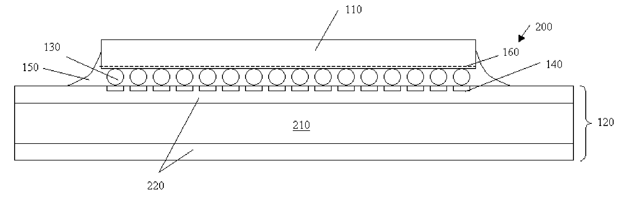
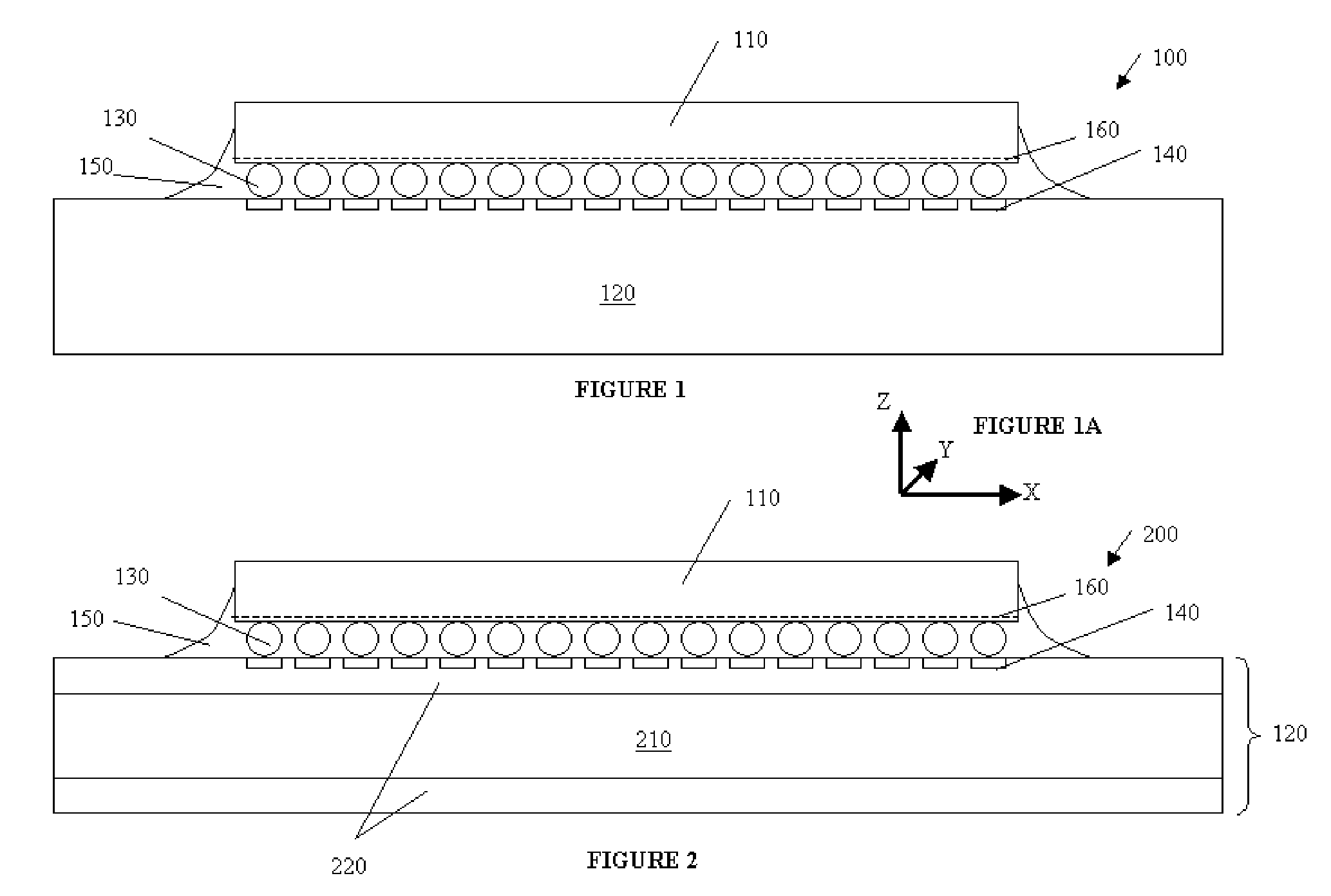
[0014] Turning initially to FIG. 1, illustrated is one embodiment of a semiconductor package device 100 constructed according to the disclosed principles. Specifically, the package device 100 includes an integrated circuit (IC) chip 110 that contains numerous active and inactive components to form one or more functional integrated circuits. In addition, the IC chip 110 is configured for mounting onto another substrate 120 using a flip-chip technique. As such, solder bumps (or other appropriate coupling components) 130 are formed on the bottom or mounting surface of the IC chip 110 in a BGA.

[0015] In the illustrated embodiment, the substrate 120 on which the IC chip 110 is mounted is a package substrate 120. More specifically, the package substrate 120 includes bonding pads (one of which is labeled 140) formed on an exterior mounting surface that faces the IC chip 110, and which are configured to receive the solder bumps 130 from the IC chip during the flip-chip mounting. Finally, a...


PUM


Abstract

Disclosed are techniques that teach the replacement of the typical organic, plastic, or ceramic package substrate used in semiconductor package devices with a low-CTE package substrate. In one embodiment, a semiconductor device implementing the disclosed techniques is provided, where the device comprises an integrated circuit chip having at least one coupling component formed on an exterior surface thereof. Also, the device includes a package substrate having a mounting surface with bonding pads that are configured to receive the at least one coupling component. In such embodiments, the package substrate is selected or manufactured such that it has a coefficient of thermal expansion in a direction perpendicular to its mounting surface that is less than approximately twice a coefficient of thermal expansion along a plane parallel to its mounting surface.

Description

TECHNICAL FIELD [0001] This disclosure relates generally to manufacturing techniques for semiconductor devices, and more particularly to low CTE substrates for use with low-k flip-chip semiconductor package devices. BACKGROUND [0002] The packaging of integrated circuit (IC) chips is one of the most important steps in the manufacturing process, contributing significantly to their overall cost, performance and reliability. As semiconductor devices reach higher levels of integration, packaging technologies have become critical. Packaging of the IC chip accounts for a considerable portion of the cost of producing the device, and failure of the package leads to costly yield reduction. [0003] Continued decrease in semiconductor device feature size has led to a significant increase in semiconductor device density, which places increased emphasis on device or package I / O capabilities. The metal connections, which connect the integrated circuit to other circuits or to system components, have...

Claims


Application Information

Patent Timeline
Patent Type & Authority Applications(United States)
IPC IPC(8): H01L21/44H01L23/48
CPCH01L21/563H01L23/14H01L23/15H01L23/3128H01L23/3735H01L2224/16H01L2924/01322H05K3/4602H05K2201/068H05K2201/10674H01L2924/01019H01L2924/01037H01L2924/01068H05K1/0271H01L2224/13116H01L2224/16227H01L2224/32225H01L2224/73204H01L2224/81805H01L2224/92125H01L2224/16225H01L2924/00
Inventor LU, SZU-WEILEE, HSIN-HUILEE, CHIEN-HSIUNLII, MIRNG-JI
Owner TAIWAN SEMICON MFG CO LTD
Why Eureka
Try Eureka