Organic light emitting diode display

Active Publication Date: 2007-01-11
LG DISPLAY CO LTD
7 Cites 196 Cited by

AI-Extracted Technical Summary

Problems solved by technology

Secondly, the reliability of the scan operation of the OLED display device of the related art decreases because an undesired voltage is applied to the gate line due to a charge remaining in control nodes which control the output of the scan drive circuit 12.
Thirdly,...

Method used

[0057] In this way, the scan drive circuit 102 and the reset drive circuit 106 that are formed embedded together with the pixel array in the OLED panel 103, thus circuit cost can be minimized and a process of forming a circuit or adhering to the pixel array substrate is not required.
[0065] In other words, the stress of the second transistor T2 for the first half frame period is recovered during the second half frame period, thereby preventing deterioration of the second transistor T2, i.e., the OLED drive device, so that it is possible to improve the reliability of the OLED drive circuit.
[0085] In this way, the scan drive circuit 102 and the rese...

Benefits of technology

[0022] An advantage of the present invention is to provide an organic light emitting diode display device that prevents a characteristic change of a device that drives the organic light emitting diode and for improving the reliability of the device.
[0023] Another advantage of the present invention is to provide an organic light emitting diode display device that improves the reliability of driving the OLED by periodically discharging a residual charge of a scan line and a control node within a scan drive circuit.
[0024] Another advantage of the present invention is to provide an organic light emitting diode display device that reduces the circuit cost and the fabrication process complexity.
[0025] Additional features and advantages of the invention will be set forth in the description which follows, and in part will be apparent from the description, or may be learned by practice of the invention. The objectives and other advantages of the invention will be realized and attained by the structure particularly pointed out in the written description and claims hereof as well as the appended drawings.
[0026] To achieve these and other advantages and in accordance with the purpose of the present invention, as embodied and broadly described, an organic light emitting diode display device according to an aspect of the present invention includes: a pixel array having a plurality of scan lines and a plurality of data lines that cross each other, a plurality of power voltage supply lines to which a high level power supply voltage is supplied and that are substantially parallel to the data lines, a plurality of reset lines substantially parallel to the scan lines, a plurality of organic light emitting diodes that emit light due to the high level power supply voltage from the power voltage supply line, and a plurality of organic light emitting diode drive circuits that drive the organic light emitting diode with data from the data line in response to a scan signal from the scan line and that is initialized in response to a reset signal from the reset line; a scan drive circuit that su...

Abstract

This invention relates to an organic light emitting diode display device that is adaptive for preventing a characteristic change of a device which drives the organic light emitting diode and for securing reliability of the device. The organic light emitting diode display device includes: a pixel array having a plurality of scan lines and a plurality of data lines that cross each other, a plurality of power voltage supply lines to which a high level power supply voltage is supplied and that are substantially parallel to the data lines, a plurality of reset lines substantially parallel to the scan lines, a plurality of organic light emitting diodes that emit light due to the high level power supply voltage from the power voltage supply line, and a plurality of organic light emitting diode drive circuits that drive the organic light emitting diode with data from the data line in response to a scan signal from the scan line and that is initialized in response to a reset signal from the reset line; a scan drive circuit that supplies the scan signal to the scan lines; a reset drive circuit that supplies the reset signal to the reset lines that initializes the organic light emitting diode drive circuit; and a data drive circuit that supplies the data to the data lines respectively, wherein the scan drive circuit and the reset drive circuit are on a substrate including the pixel array.

Application Domain

Technology Topic

Image

  • Organic light emitting diode display
  • Organic light emitting diode display
  • Organic light emitting diode display

Examples

  • Experimental program(3)

Example

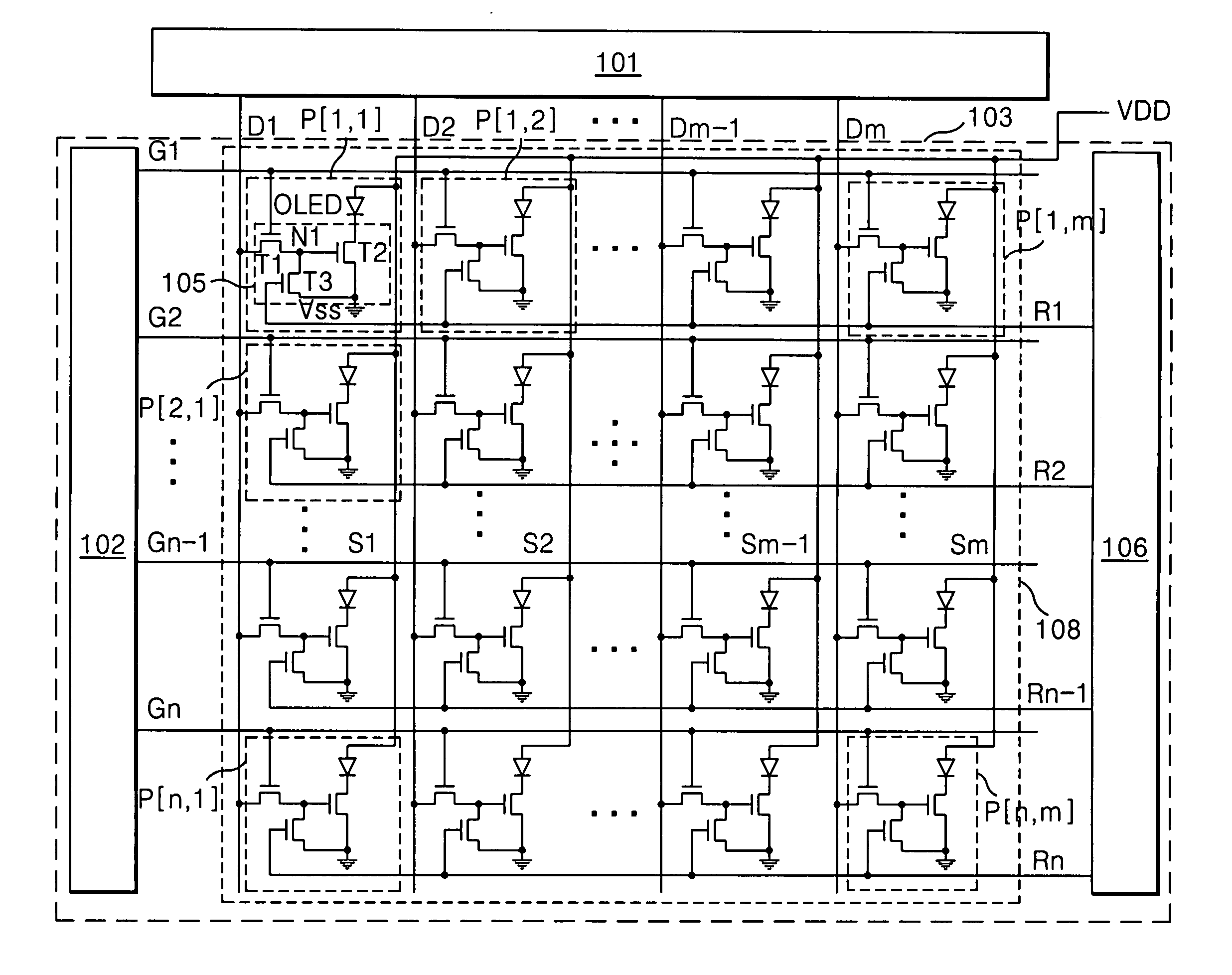
[0072]FIG. 10 is a block diagram representing a second embodiment of a scan drive circuit and a reset drive circuit of FIG. 5 or 9.
[0073] Referring to FIG. 10, the scan drive circuit 102 and the reset drive circuit 106 each includes n stages (1st to nth stages) that are connected in cascade.
[0074] In the scan drive circuit 102, a first start signal Vst1 is input to a first stage, and a pre-stage scan signal Vg_i−1 is input to second to nth stages as the start signal. The next-stage scan signal Vg_i+1 is input to the first to (n−1)th stages as a stage reset signal, and a stage reset signal from a dummy stage (not shown) is input to the nth stage. Further, each stage substantially has the same circuit configuration and shifts the first start signal Vst1 or pre-stage scan signal Vg_i in response to any one clock signal among four clock signals C1 to C4, thereby generating a scan signal having a pulse width of one horizontal period.
[0075] The second start signal Vst2 is generated later than the first start signal Vst1. Accordingly, the reset signal is delayed by a designated time versus the scan signal supplied to the scan lines G1 to Gn.

Example

[0076]FIG. 11 is a circuit diagram representing a first embodiment of the scan drive circuit and the reset drive circuit of FIG. 10 in detail.
[0077] Referring to FIG. 11, the scan drive circuit 102 includes a first transistor T1 that discharges a Q node of the stage 201 to 20n in response to the reset signal Vr_1 to Vr_n from the reset lines R1 to Rn, and the reset drive circuit 106 includes a second transistor T2 that discharges a Q node of the stage 601 to 60n in response to the scan signal Vg from the scan lines G1 to Gn.
[0078] In the scan drive circuit 102, if the start signal Vst1 is input to a set terminal S of the first stage 201, the Q node is charged and the QB node is discharged in the stage 201. Subsequently, the first scan signal Vg_1 is supplied to the first scan line G1 through a pull-up transistor T-up when the first clock signal C1 having a high logic voltage is input to the first stage 201 when the Q node is charged. At the same time, the first scan signal Vg_1 is supplied to the set terminal S of the second stage 202 to charge the Q node of the second stage 202 and to discharge a QB node of the second stage 202. Further, the first scan signal Vg_1 is applied to a gate electrode of the second transistor T2 of the reset drive circuit 106. Accordingly, the second transistor T2 is turned on by the first scan signal Vg_1 to discharge the Q node of the first stage 601 in the reset drive circuit 106.
[0079] Subsequently, the second scan signal Vg_2 generated in the second stage 202 by the second clock signal C2 is supplied to the second scan line G2 and, at the same time, is supplied to the reset terminal R of the first stage 201 as a stage reset signal. The second scan signal Vg_2 discharges the Q node of the first stage 201 and charges the QB node. Accordingly, the first scan line G1 is discharged through the pull-down transistor T_dn when the second scan signal Vg_2 is generated. Further, the second scan signal Vg_2 is applied to the gate electrode of the second transistor T2 of the second stage 602 included in the reset drive circuit 106. Accordingly, the second transistor T2 is turned on by the second scan signal Vg_2 to discharge the Q node of the second stage 602 in the reset drive circuit 106.
[0080] In the same manner, a third scan signal Vg_3 output from the third stage 203 is supplied to the third scan line G3 and, at the same time, initializes the second stage 202 as the stage reset signal. With such operations, the scan drive circuit 102 sequentially supplies the scan signal to the scan lines G1 to Gn and discharges the Q node of the reset drive circuit 106.
[0081] The reset operation of the reset drive circuit 106 is substantially made in the same manner as the foregoing scan drive circuit 102.
[0082] In the reset drive circuit 106, if the start signal Vst2 is input to a set terminal S of the first stage 601, the Q node is charged, and the QB node is discharged in the stage 601. Subsequently, the first clock signal C1 having a high logic voltage is supplied to the first reset line R1 through the pull-up transistor T-up as a first reset signal Vr_1 when the Q node is charged. At the same time, the first reset signal Vr_1 is supplied to the set terminal S of the second stage 602 to charge the Q node of the second stage 602 and to discharge a QB node of the second stage 602. Further, the first reset signal Vr_1 is applied to a gate electrode of the first transistor T1. Accordingly, the first transistor T1 is turned on by the first reset signal Vr_1 to discharge the Q node of the first stage 201 in the scan drive circuit 102.
[0083] Subsequently, the second reset signal Vr_2 generated in the second stage 602 by the second clock signal C2 is supplied to the second reset line R2 and at the same time, is supplied to the reset terminal R of the first stage 601 as a stage reset signal. The second reset signal Vr_2 discharges the Q node of the first stage 601 and charges the QB node. Accordingly, the first reset line R1 is discharged through the pull-down transistor T_dn when the second reset signal Vr_2 is generated. Further, the second reset signal Vr_2 is applied to the gate electrode of the first transistor T1 of the second stage 202 included in the scan drive circuit 102. Accordingly, the first transistor T1 is turned on by the second reset signal Vr_2 to discharge the Q node of the second stage 201 in the scan drive circuit 102.
[0084] In the same manner, a third reset signal Vr_3 output from the third stage 603 is supplied to the third reset line R3 and, at the same time, initializes the second stage 602 as the stage reset signal. With such operations, the reset drive circuit 106 sequentially supplies the reset signal to the reset lines R1 to Rn and discharges the Q node of the scan drive circuit 102.
[0085] In this way, the scan drive circuit 102 and the reset drive circuit 106 discharge the Q node with the output of another stage, thus it is possible to prevent a malfunction of the OLED caused by an excessive charge on the Q node and to improve reliability of the circuits.
[0086]FIG. 12 is a circuit diagram representing a second embodiment of the scan drive circuit and the reset drive circuit of in FIG. 10 in detail.
[0087] Referring to FIG. 12, the scan drive circuit 102 includes a third transistor T3 that discharges the scan lines G1 to Gn in response to the reset signal Vr_1 to Vr_n from the reset lines R1 to Rn, and the reset drive circuit 106 includes a fourth transistor T4 which discharges the reset lines R1 to Rn in response to the scan signals Vg_1 to Vg_n from the scan lines G1 to Gn.
[0088] A source electrode of the third transistor T3 is connected to the scan lines G1 to Gn and a drain electrode thereof is connected to a low level power supply voltage source VSS. A gate electrode of the third transistor T3 is connected to the reset lines R1 to Rn.
[0089] A source electrode of the fourth transistor T4 is connected to the reset lines R1 to Rn and a drain electrode thereof is connected to a low level power supply voltage source VSS. A gate electrode of the fourth transistor T4 is connected to the scan lines G1 to Gn.
[0090] In the scan drive circuit 102, if the start signal Vst1 is input to the first stage 201, the Q node is charged in the first stage 201 and the QB node is discharged. If the first clock signal with a high voltage is supplied to the source electrode of the pull-up transistor T-up when the Q node of the first stage 201 is charged, the first scan signal Vg_1 is supplied to the first scan line G1 and at the same time is supplied to the set terminal S of the second stage 202 as the start signal, thereby charging the Q node of the second stage 202 and discharging the QB node of the second stage 202. Further, the first scan signal Vg_1 is applied to the gate electrode of the fourth transistor T4 connected to the first reset line R1 to discharge the first reset line R1.
[0091] The second scan signal Vg_2 generated in the second stage 202 of the scan drive circuit 102 by the second clock signal C2 is supplied to the second scan line G2 and, at the same time, is supplied to the reset terminal R of the first stage 201, thereby discharging the Q node of the first stage 201 and charging the QB node of the fist stage 201. Accordingly, if the second scan signal Vg_2 is generated, the pull-down transistor T_dn of the first stage 201 is turned on to discharge the first scan line G1 to the low level power supply voltage VSS and, at the same time, the pull-up transistor T_up of the second stage 202 is turned on to charge the second scan line G2 to the voltage of the second clock signal C2. Further, the second scan signal Vg_2 is applied to the gate electrode of the fourth transistor T4 connected to the second reset line R2 to discharge the second reset line R1.
[0092] With such operations, the scan drive circuit 102 sequentially supplies the scan signals Vg_1 to Vg_n to the scan lines G1 to Gn and initializes the pre-stage stage at the same time. Further, the scan drive circuit 102 sequentially discharges the reset lines R1 to Rn.
[0093] In the reset drive circuit 106, if the start signal Vst2 is input to the first stage 601, the Q node is charge in the first stage 601 and the QB node is discharged. If the first clock signal with a high voltage is supplied to the source electrode of the pull-up transistor T-up when the Q node of the first stage 601 is charged, the first reset signal Vr_1 is supplied to the first reset line R1 and, at the same time, is supplied to the set terminal S of the second stage 602 as the start signal, thereby charging the Q node of the second stage 602 and discharging the QB node of the second stage 602. Further, the first reset signal Vr_1 is applied to the gate electrode of the third transistor T3 connected to the first scan line G1 to discharge the first scan lien G1.
[0094] The second scan signal Vg_2 generated in the second stage 602 of the scan drive circuit 106 by the second clock signal C2 is supplied to the second reset line R2 and, at the same time, is supplied to the reset terminal R of the first stage 601, thereby discharging the Q node of the first stage 601 and charging the QB node of the fist stage 601. Accordingly, if the second reset signal Vr_2 is generated, the pull-down transistor T_dn of the first stage 601 is turned on to discharge the first reset line R1 to the low level power supply voltage VSS and, at the same time, the pull-up transistor T_up of the second stage 602 is turned on to charge the second reset line R2 to the voltage of the second clock signal C2. Further, the second reset signal Vr_2 is applied to the gate electrode of the third transistor T3 connected to the second scan line G2 to discharge the second scan line G1.
[0095] With such operations, the reset drive circuit 106 sequentially supplies the reset signal Vr_1 to Vr_n to the reset lines R1 to Rn and initializes the pre-stage stage at the same time. Further, the reset drive circuit 106 sequentially discharges the scan lines G1 to Gn.

Example

[0096]FIG. 13 is a circuit diagram representing a third embodiment of the scan drive circuit and a reset drive circuit shown in FIG. 10, in detail.
[0097] Referring to FIG. 13, the scan drive circuit 102 includes a first transistor T1 that discharges the Q node of the stage 201 to 20n in response to the reset signal Vr_1 to Vr_n from the reset lines R1 to Rn; and a third transistor T3 that discharges the scan lines G1 to Gn in response to the reset signal Vr_1 to Vr_n.
[0098] The reset drive circuit 106 includes a second transistor that discharges the Q node of the stage 601 to 60n in response to the scan signal Vg from the scan lines G1 to Gns; and a fourth transistor T4 that discharges the reset lines R1 to Rn in response to the scan signals Vg_1 to Vg_n from the scan lines G1 to Gn.
[0099] A source electrode of the first transistor T1 is connected to the Q node of the stages 201 to 20n included in the scan drive circuit 102, and a drain electrode thereof is connected to the low level power supply voltage source VSS. A gate electrode of the first transistor T1 is connected to the reset lines R1 to Rn.
[0100] A source electrode of the second transistor T2 is connected to the Q node of the stages 601 to 60n included in the reset drive circuit 106, and a drain electrode thereof is connected to the low level power supply voltage source VSS. A gate electrode of the second transistor T2 is connected to the reset lines R1 to Rn.
[0101] A source electrode of the third transistor T3 is connected to the scan lines G1 to Gn, and a drain electrode thereof is connected to the low level power supply voltage source VSS. A gate electrode of the third transistor T3 is connected to the reset lines R1 to Rn.
[0102] A source electrode of the fourth transistor T4 is connected to the reset lines R1 to Rn, and a drain electrode thereof is connected to the low level power supply voltage source VSS. A gate electrode of the fourth transistor T4 is connected to the scan lines G1 to Gn.
[0103] The scan drive circuit 102 and the reset drive circuit 106 shown in FIG. 13 are an embodiment where the circuit configurations of the scan drive circuit 102 and the reset drive circuit 106 shown in FIGS. 11 and 12 are combined.
[0104] In the scan drive circuit 102, if the start signal Vst1 is input to the first stage 201, the Q node is charged in the first stage 201 and the QB node is discharged. If the first clock signal with a high voltage is supplied to the source electrode of the pull-up transistor T-up when the Q node of the first stage 201 is charged, the first scan signal Vg_1 is supplied to the first scan line G1 and at the same time is supplied to the set terminal S of the second stage 202 as the start signal, thereby charging the Q node of the second stage 202 and discharging the QB node of the second stage 202. Further, the first scan signal Vg_1 cuases the second and fourth transistors T2, T4 of the first stage 601 of the reset drive circuit 106 to be turned on, thereby discharging the Q node of the first stage 601 and discharging the first reset line R1.
[0105] The second scan signal Vg_2 generated by the second stage 202 of the scan drive circuit 102 by the second clock signal C2 is supplied to the second scan line G2 and, at the same time, is supplied to the reset terminal R of the first stage 201, thereby discharging the Q node of the first stage 201 and charging the QB node of the fist stage 201. Accordingly, if the second scan signal Vg_2 is generated, the pull-down transistor T_dn of the first stage 201 is turned on to discharge the first scan line G1 to the low level power supply voltage VSS and, at the same time, the pull-up transistor T_up of the second stage 202 is turned on to charge the second scan line G2 to the voltage of the second clock signal C2. Further, the second scan signal Vg_2 caused the second and fourth transistors T2, T4 of the second stage 602 of the reset drive circuit 106 to be turned on, thereby discharging the Q node of the second stage 602 and discharging the second reset line R2.
[0106] With such operations, the scan drive circuit 102 sequentially supplies the scan signals Vg_1 to Vg_n to the scan lines G1 to Gn and initializes the pre-stage stage at the same time. Further, the Q nodes are sequentially discharged in stages 601 to 60n of the reset drive circuit 106, and the reset lines R1 to Rn are sequentially discharged at the same time.
[0107] In the scan drive circuit 106, if the start signal Vst1 is input to the first stage 601, the Q node is charge in the first stage 601 and the QB node is discharged. If the first clock signal with a high voltage is supplied to the source electrode of the pull-up transistor T-up when the Q node of the first stage 601 is charged, the first reset signal Vr_1 is supplied to the first reset line R1 and, at the same time, is supplied to the set terminal S of the second stage 602 as the start signal, thereby charging the Q node of the second stage 602 and discharging the QB node of the second stage 602. Further, the first reset signal Vr_1 causes the first and third transistors T1, T3 of to the first stage 201 of the scan drive circuit 102 to be turned on, thereby discharging the Q node of the first stage 201 and discharging the first scan line G1.
[0108] The second reset signal Vr_2 generated in the second stage 602 of the reset drive circuit 106 by the second clock signal C2 is supplied to the second reset line R2 and, at the same time, is supplied to the reset terminal R of the first stage 601, thereby discharging the Q node of the first stage 601 and charging the QB node of the fist stage 601. Accordingly, if the second reset signal Vr_2 is generated, the pull-down transistor T_dn of the first stage 601 is turned on to discharge the first reset line R1 to the low level power supply voltage VSS and, at the same time, the pull-up transistor T_up of the second stage 602 is turned on to charge the second reset line R2 to the voltage of the second clock signal C2. Further, the second reset signal Vr_2 causes the first and third transistors T1, T3 of the second stage 202 of the scan drive circuit 102 to be turned on, thereby discharging the Q node of the first stage 202 and discharging the second scan line G2.
[0109] With such operations, the reset drive circuit 106 sequentially supplies the reset signal Vr_1 to Vr_n to the reset lines R1 to Rn and initializes the pre-stage stage at the same time. Further, the Q nodes are sequentially discharged in the stages 201 to 20n of the scan drive circuit 102 and the scan lines G1 to Gn are sequentially discharged at the same time.
[0110]FIG. 14 is a block diagram representing a third embodiment of the scan drive circuit and the reset drive circuit of FIG. 5 or 9 in detail.
[0111] Referring to FIG. 14, the reset drive circuit 306 simultaneously supplies the reset signal to adjacent two reset lines R1 to Rn, and includes n/2 number of stages that sequentially shift the reset signal.
[0112] A scan drive circuit 302 of the embodiment includes n number of stages which sequentially supply the scan signal to the scan lines G1 to Gn.
[0113] Each of the scan drive circuit 302 and the reset drive circuit 306 can be realized as in FIGS. 15 to 17.
[0114] Referring to FIG. 15, the scan drive circuit 302 includes: an eleventh transistor T11 that discharges the Q node of the (4k+1)th (k is a natural number not less than 0) stage 201, 205, . . . , 20n−3 in response to an odd number reset signal Vr_1, Vr_3, . . . , Vr_(n/2)−1; a thirteenth transistor T13 that discharges the Q node of the (4k+2)th stage 202, 206, . . . , 20n−2 in response to the odd number reset signal Vr_1, Vr_3, . . . , Vr_(n/2)−1; a fourteenth transistor T14 which discharges the Q node of the (4k+3)th stage 203, 207, . . . , 20n−1 in response to an even number reset signal Vr_2, Vr_4, . . . , Vr_(n/2); and a fifteenth transistor T15 that discharges the Q node of the (4k+4)th stage 204, 208, . . . , 20n in response to an even number reset signal Vr_2, Vr_4, . . . , Vr_(n/2).
[0115] The reset drive circuit 306 includes a twelfth transistor T12 that discharges the Q node of an odd number stage 601, 603, . . . , 60n/2−1 in response to an odd number scan signal Vg_1, Vg_3, . . . , Vr_(n−1) and a fifteenth transistor T15 that discharges the Q node of an even number stage 602, 604, . . . , 60n/2 in response to the odd number scan signal Vg_1, Vg_3, . . . , Vr_(n−1).
[0116] In the scan drive circuit 302, if the start signal Vst1 is input to a set terminal S of the first stage 201, the Q node is charged, and the QB node is discharged in the stage 201. Subsequently, the first scan signal Vg_1 is supplied to the first scan line G1 through a pull-up transistor T-up when the first clock signal C1 having a high logic voltage is input to the first stage 201 the Q node is charged. At the same time, the first scan signal Vg_1 is supplied to the set terminal S of the second stage 202 to charge the Q node of the second stage 202 and to discharge a QB node of the second stage 202. Further, the first scan signal Vg_1 is applied to a gate electrode of the twelfth transistor T12 of the reset drive circuit 306. Accordingly, the twelfth transistor T12 is turned on by the first scan signal Vg_1 to discharge the Q node of the first stage 601 in the reset drive circuit 306.
[0117] Subsequently, the second scan signal Vg_2 generated in the second stage 202 by the second clock signal C2 is supplied to the second scan line G2 and, at the same time, is supplied to the reset terminal R of the first stage 201 as a stage reset signal. The second scan signal Vg_2 discharges the Q node of the first stage 201 and charges the QB node. Accordingly, the first scan line G1 is discharged through the pull-down transistor T_dn when the second scan signal Vg_2 is generated.
[0118] A third scan signal Vg_3 output from the third stage 203 is supplied to the third scan line G3 and, at the same time, initializes the second stage 202 as the stage reset signal. The sixteenth transistor T16 is turned on to discharge the Q node that is formed in the second stage 602 of the reset drive circuit 306. With such operations, the scan drive circuit 302 sequentially supplies the scan signal to the scan lines G1 to Gn and discharges the Q node of the reset drive circuit 306.
[0119] In the reset drive circuit 306, if the start signal Vst2 is input to a set terminal S of the first stage 601, the Q node is charged and discharged in the stage 601. Subsequently, the first clock signal C1 having a high logic voltage is simultaneously supplied to the first and second reset lines R1 and R2 through the pull-up transistor T-up as a first reset signal Vr_1 when the Q node is charged. At the same time, the first reset signal Vr_1 is supplied to the set terminal S of the second stage 602 to charge the Q node of the second stage 602 and to discharge a QB node of the second stage 602. Further, the first reset signal Vr_1 is applied to a gate electrode of the eleventh and thirteenth transistors T11 and T13 of the scan drive circuit 302. Accordingly, the eleventh and thirteenth transistors T11 and T13 are turned on by the first reset signal Vr_1 to discharge the Q node of the first and second stages 201, 202 in the scan drive circuit 302.
[0120] Subsequently, the second reset signal Vr_2 generated in the second stage 602 by the third clock signal C3 is supplied to the third and fourth reset lines R3, R4 and, at the same time, is supplied to the reset terminal R of the first stage 601 as a stage reset signal. The second reset signal Vr_2 discharges the Q node of the first stage 601 and charges the QB node. Accordingly, the first reset line R1 is discharged through the pull-down transistor T_dn when the second reset signal Vr_2 is generated. Further, the second reset signal Vr_2 is applied to the gate electrode of the fourteenth and fifteenth transistors T14 and T15. Accordingly, the fourteenth and fifteenth transistors T14 and T15 are turned on by the second reset signal Vr_2 to discharge the Q node of the third and fourth stages 203, 204 in the scan drive circuit 302.
[0121] With such operations, the reset drive circuit 306 sequentially supplies the reset signal to the reset lines R1 to Rn and sequentially discharges the Q node of the scan drive circuit 302.
[0122] Referring to FIG. 16, the scan drive circuit 302 includes: a seventeenth transistor T17 that discharges the (4k+1)th scan line G1, G5, . . . , Gn−3 in response to an odd number reset signal Vr_1, Vr_3 , . . . , Vr_(n/2)−1; an eighteenth transistor T18 that discharges the (4k+2)th scan line G2, G6, . . . , Gn−2 in response to the odd number reset signal Vr_1, Vr_3, . . . , Vr_(n/2)−1; a nineteenth transistor T19 that discharges the (4k+3)th scan line G3, G7, . . . , Gn−1 in response to an even number reset signal Vr_2, Vr_4, . . . , Vr_n/2; and a twentieth transistor T20 that discharges the (4k+4)th scan line G4, G8, . . . , Gn in response to the even number reset signal Vr_2, Vr_4, . . . , Vr_n/2.
[0123] The reset drive circuit 306 includes a twelfth transistor T12 that discharges the Q node of an odd number stages 601, 603, . . . , 60n/2−1 in response to an odd number scan signals Vg_1, Vg_3, . . . , Vr_(n−1); a twenty first transistor T21 that discharges the (4k+1)th and (4k+2)th reset lines R1, R2, . . . , Rn−3, Rn−2 in response to the odd number scan signals Vg_1, Vg_3, . . . , Vg_(n/2)−1; a fifteenth transistor T15 that discharges the Q node of an even number stage 602, 604, . . . , 60n/2 in response to the odd number scan signals Vg_1, Vg_3, . . . , Vr_(n−1); and a twenty second transistor T22 that discharges the (4k+3)th and 4kth reset lines R3, R4, . . . , Rn−1, Rn in response to the odd number scan signals Vg_1, Vg_3, . . . , Vg_(n/2)−1.
[0124] In the scan drive circuit 302, if the start signal Vst1 is input to the first stage 201, the Q node is charged in the first stage 201 and the QB node is discharged. If the first clock signal of a high voltage is supplied to the source electrode of the pull-up transistor T-up when the Q node of the first stage 201 is charged, the first scan signal Vg_1 is supplied to the first scan line G1 and, at the same time, is supplied to the set terminal S of the second stage 202 as the start signal, thereby charging the Q node of the second stage 202 and discharging the QB node of the second stage 202. Further, the first scan signal Vg_1 is applied to the gate electrode of the twelfth and twenty first transistors T12, T21 to discharge the Q node of the first stage 601 in the reset drive circuit 306 and to discharge the first and second reset lines R1 and R2.
[0125] The second scan signal Vg_2 generated in the second stage 202 of the scan drive circuit 302 when the second clock signal C2 is supplied to the second scan line G2 and, at the same time, is supplied to the reset terminal R of the first stage 201, thereby discharging the Q node of the first stage 201 and charging the QB node of the fist stage 201. Accordingly, if the second scan signal Vg_2 is generated, the pull-down transistor T_dn of the first stage 201 is turned on to discharge the first scan line G1 to the low level power supply voltage VSS and, at the same time, the pull-up transistor T_up of the second stage 202 is turned on to charge the second scan line G2 to the voltage of the second clock signal C2.
[0126] The third scan signal Vg_3 output from the third stage 203 is supplied to the third scan line G2 and, at the same time, initializes the second stage 202 as the stage reset signal. The fifteenth and twenty second transistors T15, T22 are turned on to discharge the Q node in the second stage 602 of the reset drive circuit 306 and to discharge the third and fourth reset lines R3, R4. With such operations, the scan drive circuit 302 sequentially supplies the scan signals Vg_1 to Vg_n to the scan lines G1 to Gn and sequentially discharges the Q node of the reset drive circuit 306 and the reset lines R1 to Rn.
[0127] In the first stage 601 of the reset drive circuit 306, if the start signal Vst2 is input to the set terminal S, the Q node is charged in the first stage 601 and the QB node is discharged. Subsequently, the first clock signal C1 having a high logic voltage is simultaneously supplied to the first and second reset lines R1, R2 as the first reset signal Vr_1 through the pull-up transistor T-up when the Q node is charged. At the same time, the first reset signal Vr_1 is supplied to the set terminal S of the second stage 602, thereby charging the Q node of the second stage 602 and discharging the QB node of the second stage 602. Further, the first reset signal Vr_1 is applied to the gate electrode of the seventeenth and eighteenth transistors T17 and T18 of the scan drive circuit 302. Accordingly, the seventeenth and eighteenth transistors T17 and T18 are turned on by the first reset signal Vr_1 to discharge the first and second scan lines G1, G2.
[0128] Subsequently, the second scan signal Vg_2 generated in the second stage 602 by the third clock signal C3 is supplied simultaneously to the third and fourth reset lines R3, R4 and, at the same time, is supplied to the reset terminal R of the first stage 601 as the stage reset signal. The second reset signal Vr_2 discharges the Q node of the first stage 601 and charges the QB node of the fist stage 601. Accordingly, the first reset line R1 is discharged through the pull-down transistor T_dn when the second reset signal Vr_2 is generated. Further, the second reset signal Vr_2 is applied to the gate terminal of the nineteenth and twentieth transistors T19 and T20. Accordingly, the nineteenth and twentieth transistors T19 and T20 are turned on by the second reset signal Vr_2 to discharge the third and fourth scan lines G3, G4.
[0129] With such operations, the reset drive circuit 306 sequentially supplies the reset signal Vr_1 to Vr_n to the reset lines R1 to Rn/2 and sequentially discharges the scan lines G1 to Gn.
[0130] Referring to FIG. 17, the scan drive circuit 302 includes: an eleventh transistor T11 that discharges the Q node of the (4k+1)th stages 201, 205, . . . , 20n−3 in response to an odd number reset signals Vr_1, Vr_3, . . . , Vr_(n/2)−1; a thirteenth transistor T13 that discharges the Q node of the (4k+2)th stages 202, 206, . . . , 20n−2 in response to the odd number reset signals Vr_1, Vr_3, . . . , Vr_(n/2)−1; a seventeenth transistor T17 that discharges the (4k+1)th scan lines G1, G5, . . . , Gn−3 in response to the odd number reset signal Vr_1, Vr_3, . . . , Vr_(n/2)−1; an eighteenth transistor T18 that discharges the (4k+2)th scan lines G2, G6, . . . , Gn−2 in response to the odd number reset signals Vr_1, Vr_3, . . . , Vr_(n/2)−1; a fourteenth transistor T14 that discharges the Q node of the (4k+3)th stages 203, 207. . . , 20n−1 in response to an even number reset signals Vr_2, Vr_4, . . . , Vr_n/2; a sixteenth transistor T16 that discharges the Q node of the (4k+4)th stages 204, 208, . . . , 20n in response to the even number reset signals Vr_2, Vr_4, . . . , Vr_n/2; a nineteenth transistor T19 which discharges the (4k+3)th scan line G3, G7, . . . , Gn−1 in response to the even number reset signals Vr_2, Vr_4, . . . , Vr_n/2; and a twentieth transistor T20 that discharges the (4k+4)th scan line G4, G8, . . . , Gn in response to the even number reset signals Vr_2, Vr_4, . . . , Vr_n/2.
[0131] The reset drive circuit 306 includes a twelfth transistor T12 that discharges the Q node of an odd number stages 601, 603, . . . , 60n/2−1 in response to an odd number scan signals Vg_1, Vg_3, . . . , Vr_(n−1); a twenty first transistor T21 that discharges the (4k+1)th and (4k+2)th reset lines R1, R2, . . . , Rn−3, Rn−2 in response to the odd number scan signals Vg_1, Vg_3, . . . , Vg_(n/2)−1; a fifteenth transistor T15 that discharges the Q node of an even number stages 602, 604, . . . , 60n/2 in response to the odd number scan signals Vg_1, Vg_3, . . . , Vr_(n−1); and a twenty second transistor T22 that discharges the (4k+3)th and 4kth reset lines R3, R4, . . . , Rn−1, Rn in response to the odd number scan signals Vg_1, Vg_3, . . . , Vg_(n/2)−1.
[0132] In the scan drive circuit 302, if the start signal Vst1 is input to the first stage 201, the Q node is charged in the first stage 201 and the QB node is discharged. If the first clock signal with a high voltage is supplied to the source electrode of the pull-up transistor T-up when the Q node of the first stage 201 is charged, the first scan signal Vg_1 is supplied to the first scan line G1 and, at the same time, is supplied to the set terminal S of the second stage 202 as the start signal, thereby charging the Q node of the second stage 202 and discharging the QB node of the second stage 202. Further, the first scan signal Vg_1 is applied to the gate electrode of the twelfth and twenty first transistors T12, T21 to discharge the Q node of the first stage 601 in the reset drive circuit 306 and to discharge the first and second reset lines R1 and R2.
[0133] The second scan signal Vg_2 generated in the second stage 202 of the scan drive circuit 302 by the second clock signal C2 is supplied to the second scan line G2 and, at the same time, is supplied to the reset terminal R of the first stage 201, thereby discharging the Q node of the first stage 201 and charging the QB node of the fist stage 201. Accordingly, if the second scan signal Vg_2 is generated, the pull-down transistor T_dn of the first stage 201 is turned on to discharge the first scan line G1 to the low level power supply voltage VSS and, at the same time, the pull-up transistor T_up of the second stage 202 is turned on to charge the second scan line G2 to the voltage of the second clock signal C2.
[0134] The third scan signal Vg_3 output from the third stage 203 is supplied to the third scan line G2 and, at the same time, initializes the second stage 202 as the stage reset signal. The fifteenth and twenty second transistors T15, T22 are turned on to discharge the Q node in the second stage 602 of the reset drive circuit 306 and to discharge the third and fourth reset lines R3, R4. With such operations, the scan drive circuit 302 sequentially supplies the scan signals Vg_1 to Vg_n to the scan lines G1 to Gn and sequentially discharges the Q node of the reset drive circuit 306 and the reset lines R1 to Rn.
[0135] In the first stage 601 of the reset drive circuit 306, if the start signal Vst2 is input to the set terminal S, the Q node is charged in the first stage 601 and the QB node is discharged. Subsequently, the first clock signal C1 having a high logic voltage is simultaneously supplied to the first and second reset lines R1, R2 as the first reset signal Vr_1 through the pull-up transistor T-up when the Q node is charged. At the same time, the first reset signal Vr_1 is supplied to the set terminal S of the second stage 602, thereby charging the Q node of the second stage 602 and discharging the QB node of the second stage 602. Further, the first reset signal Vr_1 is applied to the gate electrode of the eleventh, thirteenth, seventeenth and eighteenth transistors T11, T13, T17 and T18 of the scan drive circuit 302. Accordingly, the eleventh, thirteenth, seventeenth and eighteenth transistors T11, T13, T17 and T18 are turned on by the first reset signal Vr_1 to discharge the Q nodes of the first and second stages 201, 202 in the scan drive circuit 302 and to discharge the first and second scan lines G1, G2.
[0136] Subsequently, the second scan signal Vg_2 generated in the second stage 602 by the third clock signal C3 is supplied simultaneously to the third and fourth reset lines R3, R4 and, at the same time, is supplied to the reset terminal R of the first stage 601 as the stage reset signal. The second reset signal Vr_2 discharges the Q node of the first stage 601 and charges the QB node of the fist stage 601. Accordingly, the first reset line R1 is discharged through the pull-down transistor T_dn when the second reset signal Vr_2 is generated. Further, the second reset signal Vr_2 is applied to the gate terminal of the fourteenth, sixteenth, nineteenth and twentieth transistors T14, T16, T19 and T20. Accordingly, the fourteenth, sixteenth, nineteenth and twentieth transistors T14, T16, T19 and T20 are turned on by the second reset signal Vr_2 to discharge the Q nodes of the third and fourth stages 203, 204 in the scan drive circuit 302 and to discharge the third and fourth scan lines G3, G4 at the same time.
[0137] With such operations, the reset drive circuit 306 sequentially supplies the reset signal Vr_1 to Vr_n to the reset lines R1 to Rn/2 and sequentially discharges the Q nodes of the scan drive circuit 302 and the scan lines G1 to Gn.
[0138] As described above, the OLED display device according to the present invention can improve the reliability of the OLED drive circuit by preventing the characteristic change caused by the deterioration of the OLED drive device, especially, the drive transistor, and has the advantage of being thin and reducing cost by way of embedding the scan drive circuit and the reset drive circuit in the organic light emitting diode panel.
[0139] Further, the OLED display device according to the present invention discharges the Q nodes of the scan drive circuit and reset drive circuit and the scan lines and reset lines once again by use of the output of the drive circuits which are different from each other, thereby solving a reliability problem due to deterioration of the circuit caused by a partial charge that is generated upon driving.
[0140] It will be apparent to those skilled in the art that various modifications and variation can be made in the present invention without departing from the spirit or scope of the invention. Thus, it is intended that the present invention cover the modifications and variations of this invention provided they come within the scope of the appended claims and their equivalents.

PUM

no PUM

Description & Claims & Application Information

We can also present the details of the Description, Claims and Application information to help users get a comprehensive understanding of the technical details of the patent, such as background art, summary of invention, brief description of drawings, description of embodiments, and other original content. On the other hand, users can also determine the specific scope of protection of the technology through the list of claims; as well as understand the changes in the life cycle of the technology with the presentation of the patent timeline. Login to view more.

Similar technology patents

Classification and recommendation of technical efficacy words

Why Eureka
Try Eureka