Electronic component package including joint material having higher heat conductivity

a technology of electronic components and joint materials, applied in the direction of manufacturing tools, welding/cutting media/materials, welding apparatus, etc., can solve the problems of preventing efficient heat transfer and generating voids along the contact surfaces of joint materials, and achieve the effect of contributing to an effective heat transfer

Inactive Publication Date: 2007-01-18
FUJITSU LTD
View PDF28 Cites 13 Cited by
  • Summary
  • Abstract
  • Description
  • Claims
  • Application Information

AI Technical Summary

Benefits of technology

[0006] It is accordingly an object of the present invention to provide an electronic component package reliably contributing to an effective heat transfer. I

Problems solved by technology

Such an addition of flux to the solder material, however, results in the generation of voids along the contact surfaces of the joint material with the

Method used


Image

  • Electronic component package including joint material having higher heat conductivity
  • Electronic component package including joint material having higher heat conductivity
  • Electronic component package including joint material having higher heat conductivity

Examples


Embodiment Construction

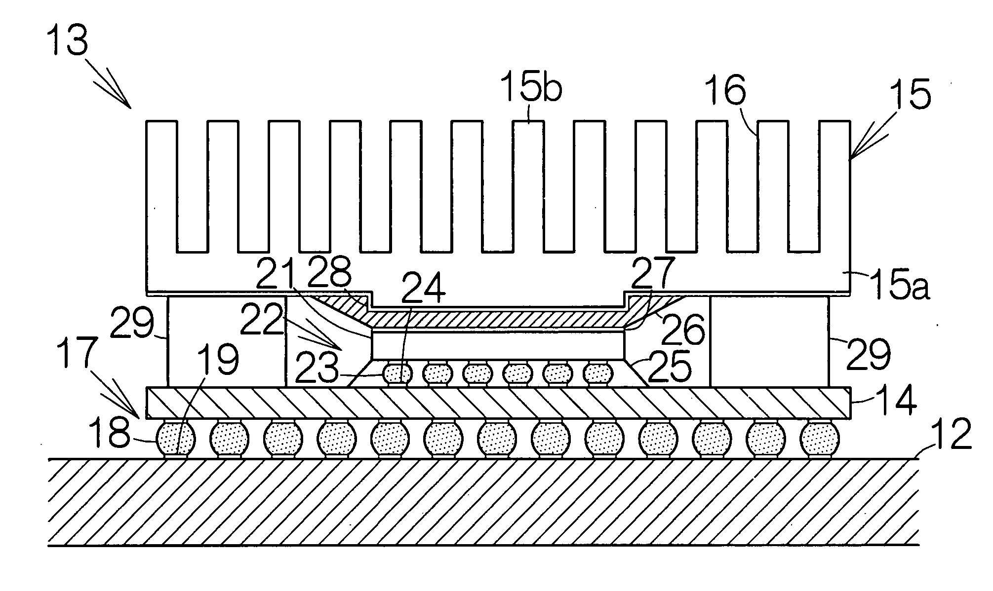
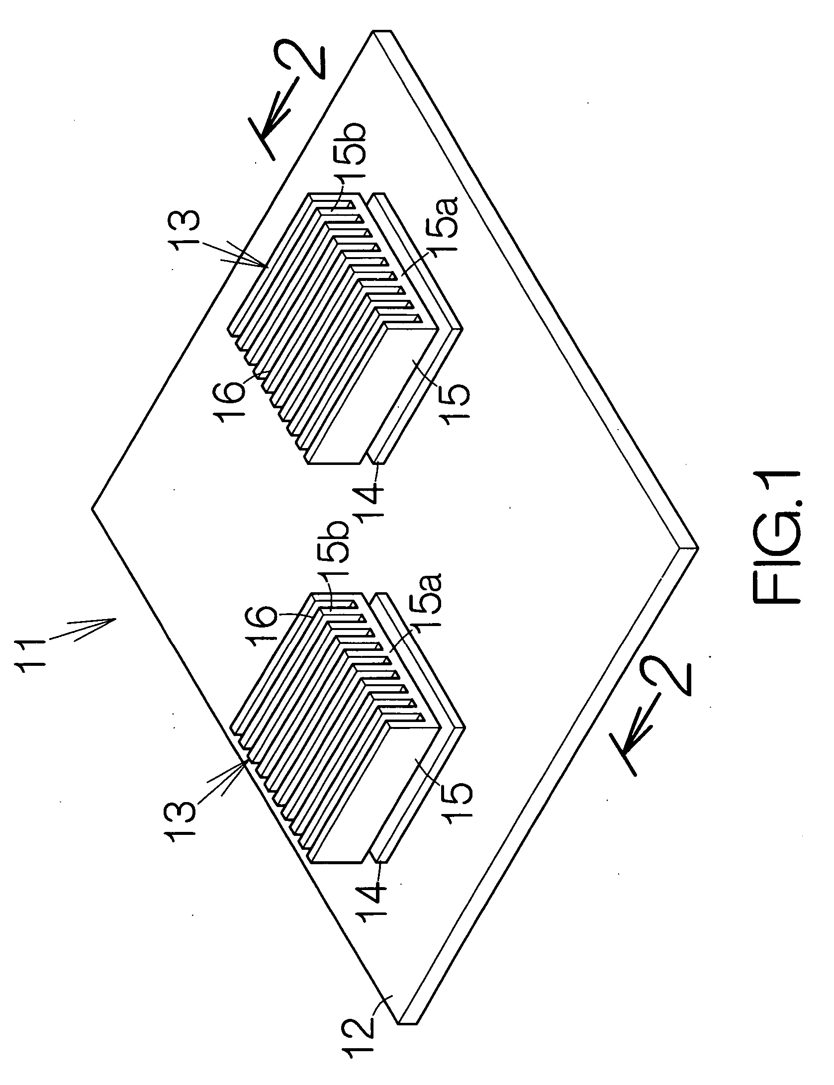
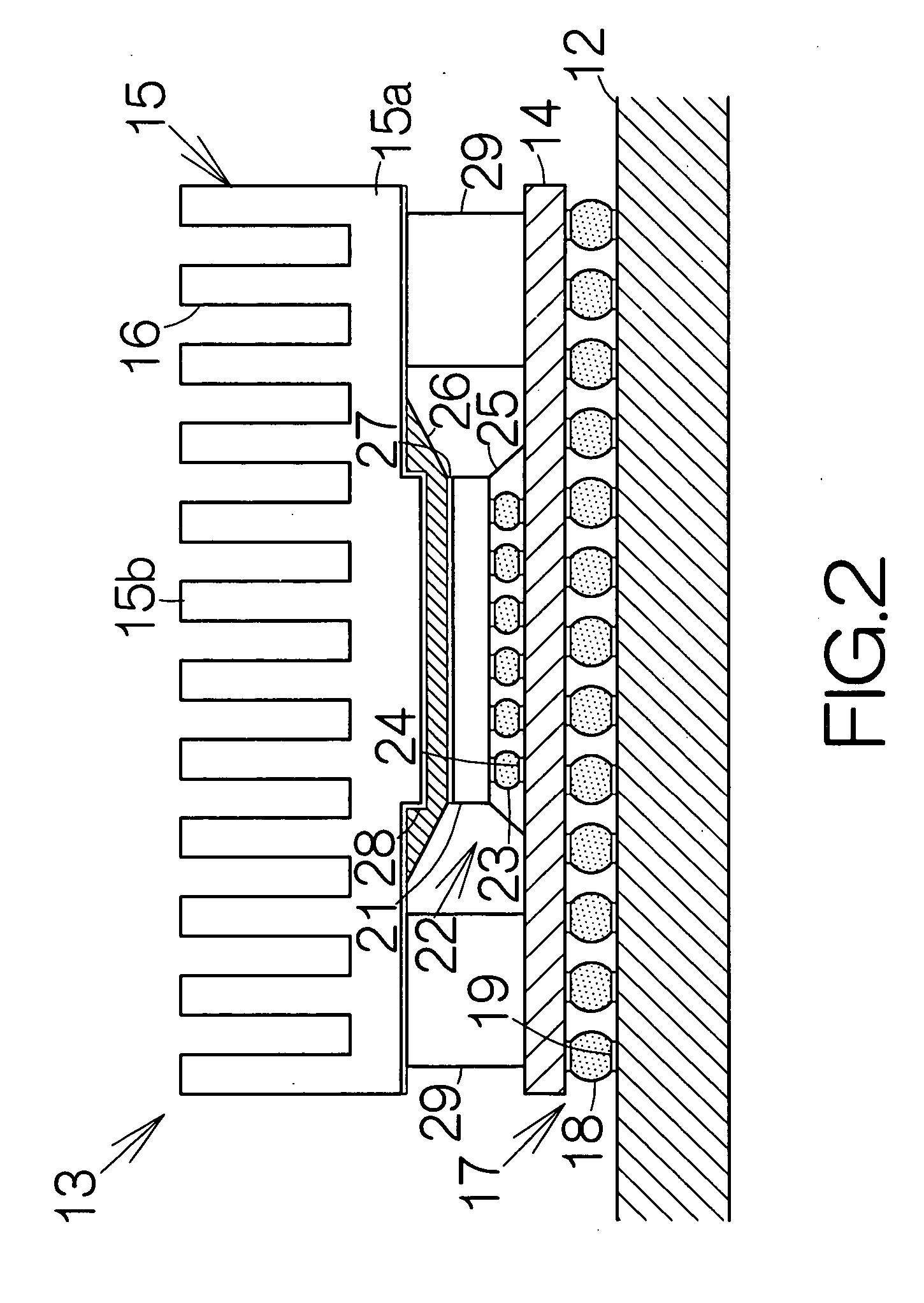
[0024]FIG. 1 schematically illustrates the structure of a motherboard 11. The motherboard 11 includes a large-sized printed wiring board 12. An electronic component package or packages 13 is mounted on the front surface of the printed wiring board 12. The individual electronic component packages 13 include a small-seized printed wiring board 14 mounted on the front surface of the printed wiring board 12. A resinous or ceramic substrate may be utilized for the printed wiring board 14, for example.

[0025] A heat conductive member or heat sink 15 is received on the printed wiring board 14. The heat sink 15 includes a plate-shaped main body or heat receiver 15a and fins 15b standing upright in a vertical direction from the heat receiver 15a. The fins 15b extend in parallel with one another. Air passages 16 are thus defined between the individual adjacent pairs of the fins 15b. The electronic component package 13 of this type enables an efficient heat radiation from the fins 15b when air...


PUM

PropertyMeasurementUnit
Temperatureaaaaaaaaaa
Electrical conductivityaaaaaaaaaa
Electrical conductoraaaaaaaaaa

Abstract

An electronic component is mounted on the surface of a printed wiring board. A heat conductive member is received on the surface of the electronic component. A joint material is interposed between the electronic component and the heat conductive member. The joint material is made of material containing Ag in a range exceeding 3 wt % and In. The inventors have demonstrated that voids decrease at the boundary between the joint material and the electronic component as well as at the boundary between the joint material and the heat conductive member as the content of Ag increases in the overall weight of the joint material. The joint material is allowed to enjoy a higher heat conductivity as compared with a conventional solder material. The joint material allows the heat conductive member to efficiently receive heat from the electronic component.

Description

BACKGROUND OF THE INVENTION [0001] 1. Field of the Invention: [0002] The present invention relates to an electronic component package including a printed wiring board, an electronic component such as a LSI (Large-Scale Integrated circuit) chip mounted on the upper surface of the printed wiring board, and a heat conductive member received on the upper surface of the electronic component on the printed wiring board. [0003] 2. Description of the Prior Art: [0004] An electronic component package often includes a LSI chip mounted on a printed wiring board. A heat conductive member such as a heat sink is received on the upper surface of the LSI chip. For example, a joint material is interposed between the LSI chip and the heat sink, as disclosed in Japanese Patent Application Publication 2000-012748. The joint material is made of a solder material, for example. Sn-Pb is employed as the solder material, for example. [0005] An activator such as flux is added to the solder material such as S...

Claims


Application Information

Patent Timeline
IPC IPC(8): H01L23/34
CPCB23K35/26B23K35/3006H01L2924/15311H01L2224/73253H01L2224/73204H01L2224/32225B23K35/3601B23K2201/40B32B15/01B32B15/018C22C28/00H01L23/3735H01L23/3736H01L24/32H01L2224/16225H01L2924/00H01L2924/01322H01L2924/15787H01L2924/14H01L2224/05573H01L2224/05568H01L2924/00014B23K2101/40H01L2224/05599H01L23/36
Inventor NAKAMURA, NAOAKIYOSHIMURA, HIDEAKIFUKUZONO, KENJISATO, TOSHIHISA
Owner FUJITSU LTD
Why Eureka
Try Eureka