Enhancing the width of polycrystalline grains with mask

Active Publication Date: 2007-01-18
THE TRUSTEES OF COLUMBIA UNIV IN THE CITY OF NEW YORK
View PDF99 Cites 41 Cited by
  • Summary
  • Abstract
  • Description
  • Claims
  • Application Information

AI Technical Summary

Benefits of technology

[0008] The present invention overcomes the above-mentioned problems by providing a mask having a row of point-type areas (e.g., diamond and/or dot patterned opaque regions) provided thereon. Such mask pattern that uses closely spaced circular or diamond-shaped areas is utilized in lieu of the straight slits in a

Problems solved by technology

The width 47 of the grain (perpendicular to the direction of the crystalline structure), however, is not very easily controlled.
In

Method used


Image

  • Enhancing the width of polycrystalline grains with mask
  • Enhancing the width of polycrystalline grains with mask
  • Enhancing the width of polycrystalline grains with mask

Examples


Example

[0021] Throughout the FIGS., the same reference numerals and characters, unless otherwise stated, are used to denote like features, elements, components or portions of the illustrated embodiments. Moreover, while the present invention will now be described in detail with reference to the FIGS., it is done so in connection with the illustrative embodiments.

DETAILED DESCRIPTION OF THE PREFERRED EMBODIMENTS

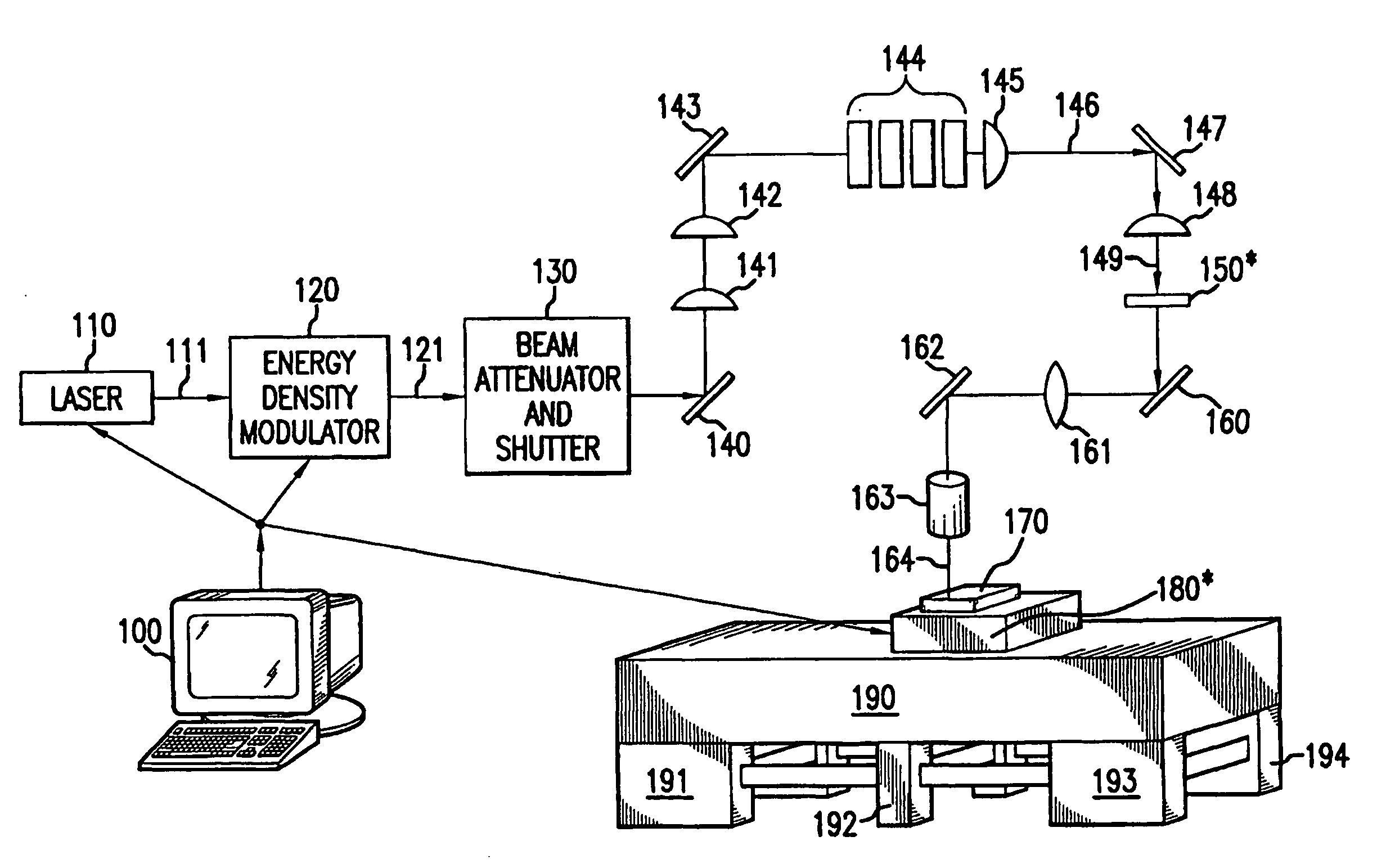
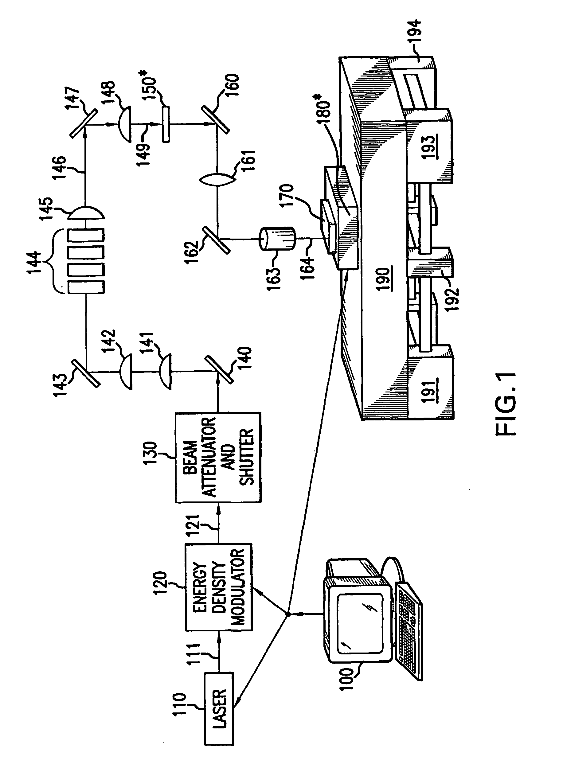
[0022] Referring to FIGS. 5-7, a presently preferred embodiment of the present invention will be described. This embodiment utilizes an exemplary mask pattern according to the present invention which uses preferably closely spaced circular or diamond-shaped areas in order to produce a microstructure with wider areas of limited number of grains provided therein. Those skilled in the art should understand that the systems, methods, and masks according to the present invention are applicable not only to single-shot motion SLS processes and systems, but also to thin films that have bee...


PUM

PropertyMeasurementUnit
Timeaaaaaaaaaa
Thicknessaaaaaaaaaa
Widthaaaaaaaaaa

Abstract

A system, method and masking arrangement are provided of enhancing the width of polycrystalline grains produced using sequential lateral solidification using a modified mask pattern is disclosed. One exemplary mask pattern employs rows of diamond or circular shaped areas in order to control the width of the grain perpendicular to the direction of primary crystallization.

Description

FIELD OF THE INVENTION [0001] The present invention relates to semiconductor processing techniques, and more particularly, techniques for fabricating semiconductors suitable for use as thin-film transistor (“TFT”) devices. BACKGROUND INFORMATION [0002] During the past several years, sequential lateral solidification (“SLS”) techniques have been developed to generate quality large grained polycrystalline thin films, e.g., silicon films, having a substantially uniform grain structure. For example, in U.S. Pat. No. 6,322,625, issued to Im and U.S. patent application Ser. No. 09 / 390,537 (the “'537 application”), the entire disclosures of which are incorporated herein by reference, particularly advantageous apparatus and methods for growing large grained polycrystalline or single crystal silicon structures using energy-controllable laser pulses and small-scale translation of a silicon sample to implement sequential lateral solidification have been described. As described in these patent ...

Claims


Application Information

Patent Timeline
IPC IPC(8): H01L21/20B23K26/00H01L21/26C30B1/00H01LH01L21/36
CPCB23K26/0656H01L21/02532H01L21/0268H01L21/02686Y10S117/904H01L21/268H01L27/1285H01L27/1296H01L29/04H01L21/02691B23K26/066
Inventor IM, JAMES S.
Owner THE TRUSTEES OF COLUMBIA UNIV IN THE CITY OF NEW YORK
Why Eureka
Try Eureka