Field emission device and method for manufacturing same

Active Publication Date: 2007-01-18
TSINGHUA UNIV +1
View PDF8 Cites 11 Cited by
  • Summary
  • Abstract
  • Description
  • Claims
  • Application Information

AI Technical Summary

Benefits of technology

[0010] The field emission device of the described embodiment has several advantages. A wide range of materials can be used in the constructio

Problems solved by technology

However, the surfaces of carbon nanotubes tend to be covered in the paste material and are therefore unable to combine with the cathode substrate directly, as a result it is difficult to control emittion state of carbon nanotubes using a cathode substrate.
Furthermore, orientation of tips of carbon nanotubes when used as emitters is inconsistent, so it is difficult to control uniformity and stability of a carbon nanotubes field emission device.
However, the above-described

Method used


Image

  • Field emission device and method for manufacturing same
  • Field emission device and method for manufacturing same
  • Field emission device and method for manufacturing same

Examples


Embodiment Construction

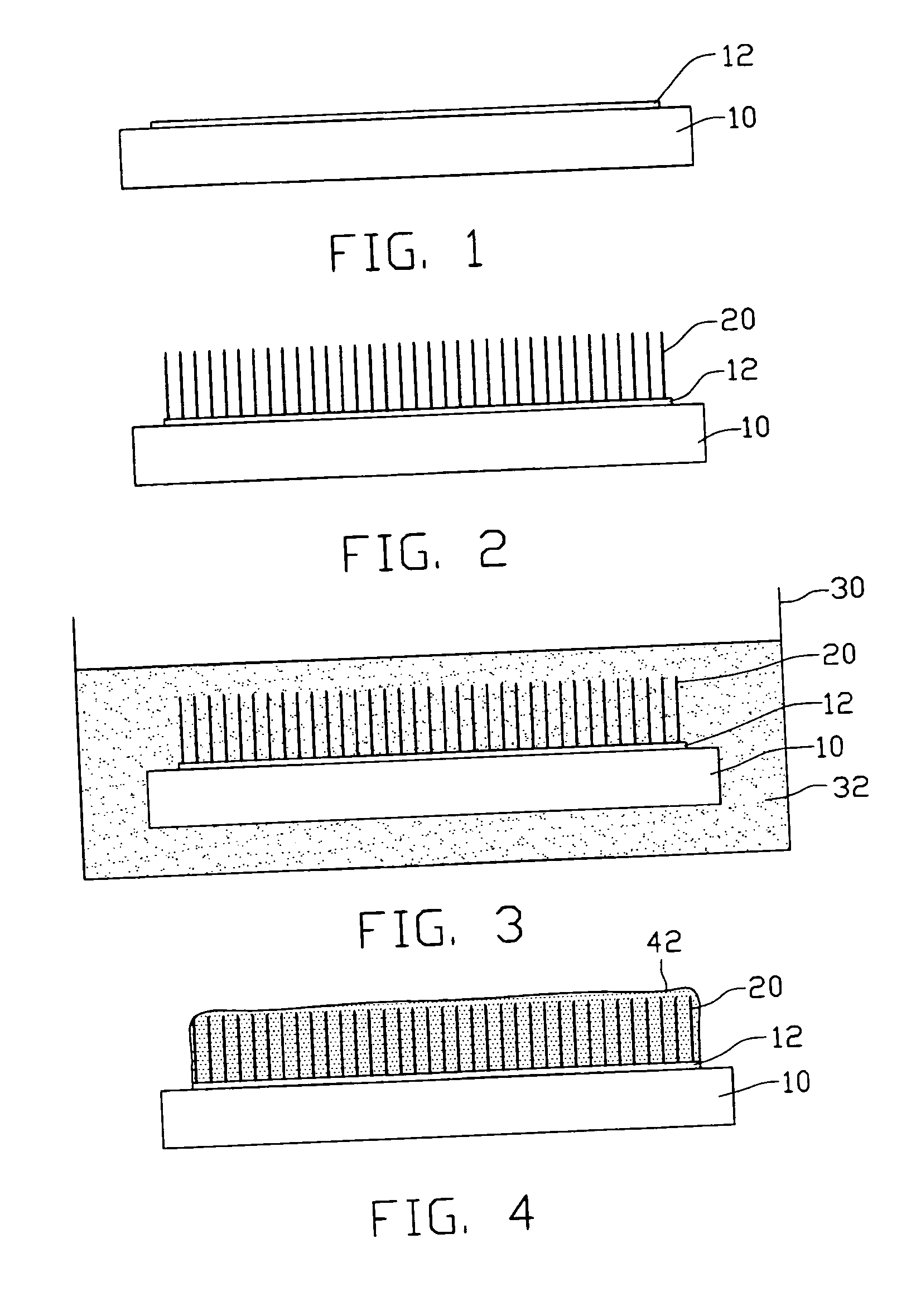
[0020] Reference will now be made to the drawings to describe embodiments of the present field emission device and method for manufacturing the same in detail.

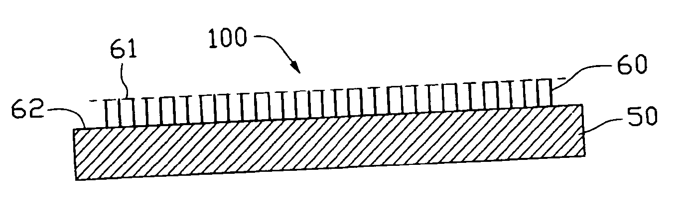
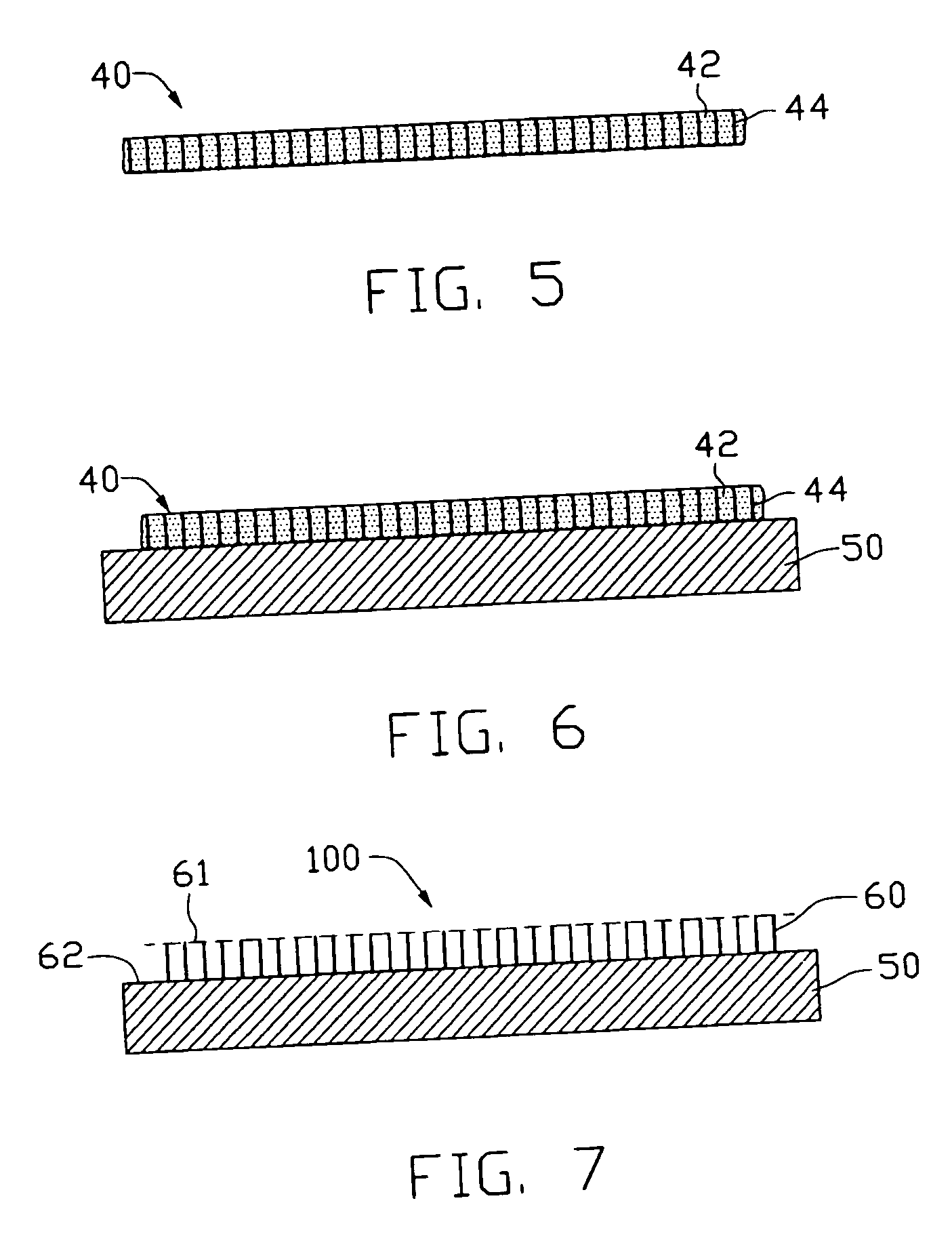
[0021] Referring to FIG. 7, a field emission device 100 according to a preferred embodiment is provided. The field emission device based on carbon nanotube array 100 includes a cathode substrate 50 and a carbon nanotube array slice 60.

[0022] The cathode substrate 50 can be made of silicon, aluminum or other metals. The cathode substrate 50 also can be indium tin oxide (ITO) glass or a non-conducting plate comprised of glass or plastic having an electrically conductive layer thereon where the electrically conductive layer is a silver-containing layer. In the first embodiment the cathode substrate 50 is made of silicon.

[0023] The carbon nanotube array slice 60 is manufactured by transversely slicing a carbon nanotube array, which will be described in detail later. A thickness of the carbon nanotube array slice 60 is in the ra...


PUM


Abstract

A field emission device, including: a cathode substrate; a carbon nanotube array slice attached on the cathode substrate, the carbon nanotube array slice including a plurality of carbon nanotube segments arranged approximately parallel to each other, the carbon nanotube segments each having a first end and an opposite second end, the first ends thereof terminating at a common plane, and the second ends thereof being electrically connected to the cathode plant. A method for manufacturing the field emission devices based on carbon nanotube array is also provided.

Description

BACKGROUND [0001] 1. Technical Field [0002] The present invention generally relates to field emission devices, and more particularly to a field emission device based on carbon nanotube array. The present invention also relates to a method for manufacturing field emission devices. [0003] 2. Discussion of Related Art [0004] Carbon nanotubes produced by arc discharge between graphite rods were first discovered and reported in an article by Sumio Iijima entitled “Helical Microtubules of Graphitic Carbon” (Nature, Vol. 354, Nov. 7, 1991, pp. 56-58). Carbon nanotubes can transmit an extremely high electrical current and emit electrons easily at a very low voltage of less than 100 volts, which makes them a very promising potential material for field emission applications. [0005] A conventional carbon nanotubes field emission device includes a cathode substrate and a carbon nanotubes layer formed thereon and functioning as an emitter. Field emission devices are widely used for field emissio...

Claims


Application Information

Patent Timeline
IPC IPC(8): H01J1/00
CPCH01J1/304H01J2329/00H01J9/025
Inventor HUANG, HUAWEI, YANGWU, YANGLIU, LIANGLIU, CHANG-HONGFAN, SHOU-SHAN
Owner TSINGHUA UNIV
Why Eureka
Try Eureka