OLED device with improved efficiency and robustness

a light-emitting diode and oled technology, applied in the direction of organic semiconductor devices, discharge tubes/lamp details, discharge tubes luminescnet screens, etc., can solve the problems of limiting the efficiency of oled devices, inefficiency in extracting photons generated by, and the majority of photons generated by recombination process are actually trapped in devices, so as to improve the robustness and performance of oled devices, and reduce manufacturing costs

Active Publication Date: 2007-01-18
GLOBAL OLED TECH
View PDF25 Cites 69 Cited by
  • Summary
  • Abstract
  • Description
  • Claims
  • Application Information

AI Technical Summary

Benefits of technology

[0021] The present invention has the advantage that it improves the r...

Problems solved by technology

It has been found, however, that one of the key factors that limits the efficiency of OLED devices is the inefficiency in extracting the photons generated by the electron-hole recombination out of the OLED devices.
Due to the high optical indices of the organic materials used, most of the photons generated by the recombination process are actually trapped in the devices due to total internal reflection.
However, for very large devices, the substrate 10 or cover 12, even when composed of rigid materials like glass and employing materials in the gap 32, can bend slightly and cause the inside of the cover 12 or gap materials to contact or press upon the thin-film layers of materials 16, possibly damaging them and reducing the utility of the OLED device.
Such an application does not, however, provide protection to thin-film layers of materials in an OLED device.
However, in this design, any thin-film layers of materials are not protected when the cover is stressed.
Moreover, the sealing material will reduce the transparency of the device and requires additional manufacturing steps.
However, columnar spacers are formed lithographically and require complex processing steps and expensive materials.
Moreover, this design is applied to liquid crystal devices and does not provide protection to thin-film structures deposited on a substrate.
This design doe...

Method used


Image

  • OLED device with improved efficiency and robustness
  • OLED device with improved efficiency and robustness
  • OLED device with improved efficiency and robustness

Examples


Embodiment Construction

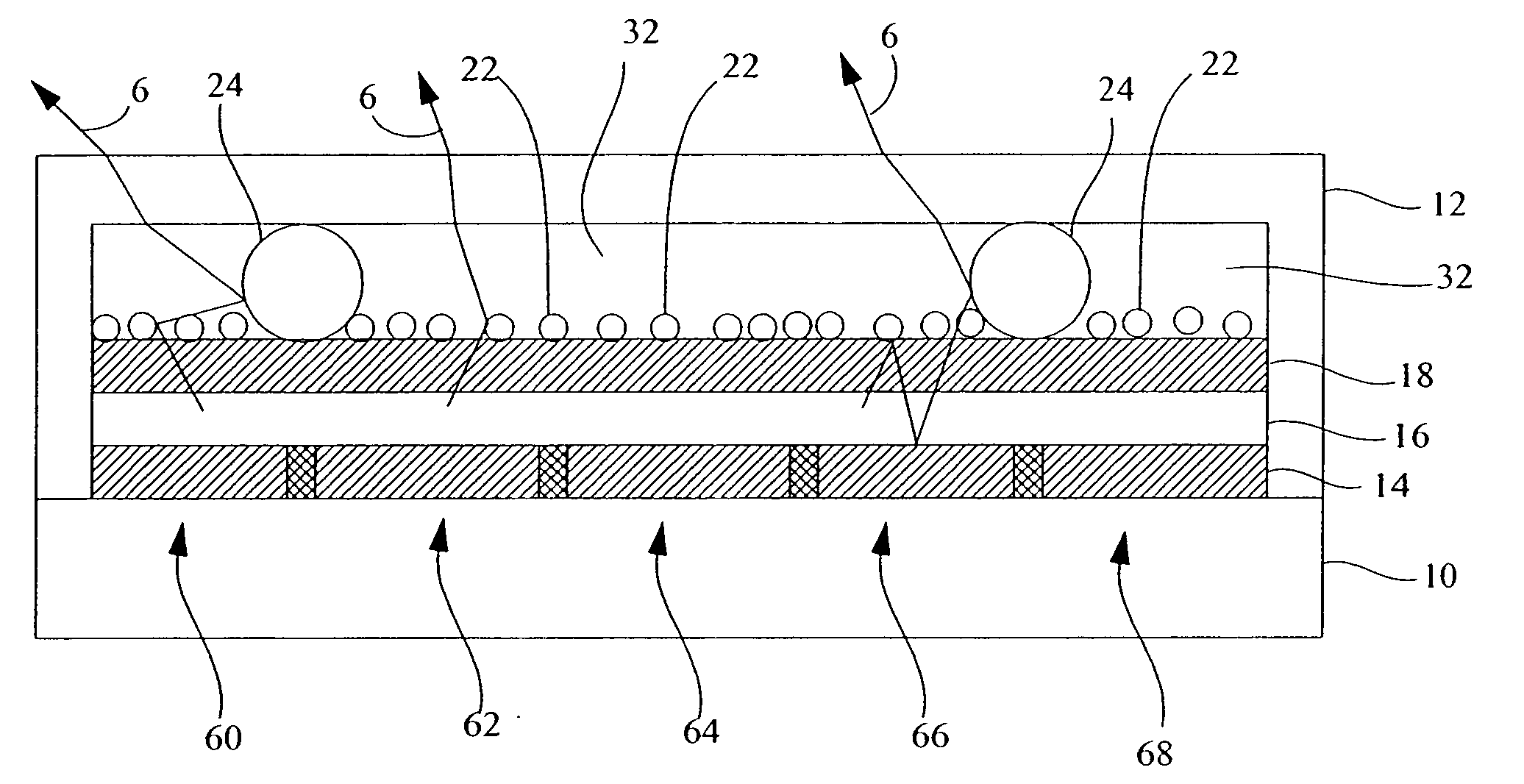
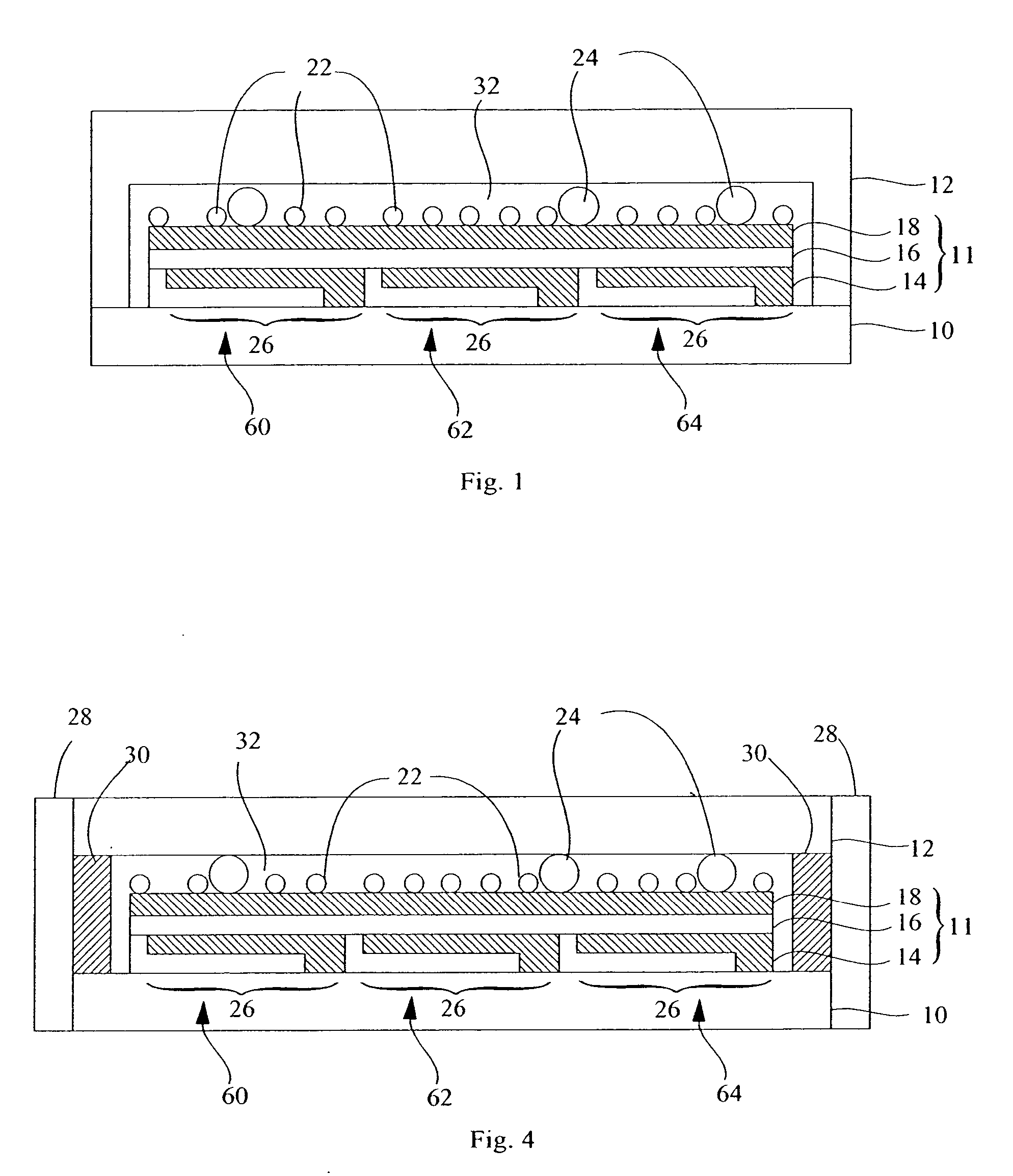
[0032] Referring to FIG. 1, in accordance with the present invention an organic light-emitting diode (OLED) device comprises a substrate 10; an OLED 11 formed on the substrate 10 comprising a first electrode 14 formed over the substrate, one or more layers of organic material 16, one of which is light emitting, formed over the first electrode 14, and a transparent second electrode 18 formed over the one or more layers of organic material 16, the transparent second electrode and layer(s) of organic light-emitting material having a first refractive index range; a transparent cover 12 provided over the OLED 11 through which light from the OLED is emitted, the cover having a second refractive index; separately formed spacer element particles 24 having a first average size distributed above the transparent second electrode 18, providing spacing between the transparent second electrode 18 and the cover 12, and forming a transparent gap 32 between the transparent second electrode and the c...


PUM


Abstract

An organic light-emitting diode (OLED) device, comprising: a substrate; an OLED formed on the substrate comprising a first electrode formed over the substrate, one or more layers of organic material, one of which emits light, formed over the first electrode, and a transparent second electrode formed over the one or more layers of organic material, the transparent second electrode and layer(s) of organic light-emitting material having a first refractive index range; a transparent cover provided over the OLED through which light from the OLED is emitted, the cover having a second refractive index; separately formed spacer element particles having a first average size distributed above the transparent second electrode, providing spacing between the transparent second electrode and the cover, and forming a transparent gap between the transparent second electrode and the cover, the transparent gap having a third refractive index lower than each of the first refractive index range and second refractive index; and separately formed light-scattering element particles distributed over the second electrode between the spacer element particles, having a second average size smaller than the first size and for scattering light emitted by the light-emitting layer.

Description

FIELD OF THE INVENTION [0001] The present invention relates to organic light-emitting diode (OLED) devices, and more particularly, to OLED device structures for improving light output, improving robustness, and reducing manufacturing costs. BACKGROUND OF THE INVENTION [0002] Organic light-emitting diodes (OLEDs) are a promising technology for flat-panel displays and area illumination lamps. The technology relies upon thin-film layers of materials coated upon a substrate and employing a cover affixed to the substrate around the periphery of the OLED device. The thin-film layers of materials can include, for example, organic materials, electrodes, conductors, and silicon electronic components as are known and taught in the OLED art. The cover includes a cavity to avoid contacting the cover to the thin-film layers of materials when the cover is affixed to the substrate. [0003] OLED devices generally can have two formats known as small molecule devices such as disclosed in U.S. Pat. No....

Claims


Application Information

Patent Timeline
IPC IPC(8): H05B33/00H05B33/02
CPCB82Y20/00B82Y30/00H01L51/525H01L2251/5369H01L51/5268H01L51/5275H01L2251/5315H01L51/5259H10K50/8428H10K50/854H10K50/858H10K2102/3026H10K2102/331
Inventor COK, RONALD S.TUTT, LEE W.
Owner GLOBAL OLED TECH
Why Eureka
Try Eureka