Check patentability & draft patents in minutes with Patsnap Eureka AI!

Interposer including air gap structure, methods of forming the same, semiconductor device including the interposer, and multi-chip package including the interposer

a semiconductor device and interposer technology, applied in the direction of solid-state devices, semiconductor/solid-state device details, instruments, etc., can solve the problems of affecting the overall operation speed of the semiconductor device, affecting the fabrication of integrated circuits operating at higher speed, and affecting the operation of the integrated circuit. , to achieve the effect of reducing the capacitance, reducing the capacitance, and improving the operation reaction speed

Inactive Publication Date: 2007-01-18
SAMSUNG ELECTRONICS CO LTD
View PDF2 Cites 9 Cited by
  • Summary
  • Abstract
  • Description
  • Claims
  • Application Information

AI Technical Summary

Benefits of technology

[0018] Example embodiments of the present invention provide an interposer of a semiconductor device with a decreased capacitance by reducing a dielectric constant of an interposer insulating layer.
[0019] Example embodiments of the present invention also provide a semiconductor device with an improved operation reaction speed by decreasing a capacitance using an interposer insulating layer.
[0020] Example embodiments of the present invention provide a multi-chip package with a faster operation reaction speed, requiring a smaller installation area.

Problems solved by technology

Thus, the reaction speed of overall operation of the semiconductor device may be slower.
In the case of a multi-chip package in which several semiconductor chips are connected as a single semiconductor device, a capacitance loading between the metal interconnects that connect the semiconductor chips may become an issue.
The capacitance loading problem caused by the metal interconnects may impede fabrication of integrated circuits operating at higher speed.
Moreover, as shown in FIG. 2, when semiconductor chips are connected via metal interconnects on the substrates, an area occupied by the multi-chip package may be enlarged, which may increase manufacturing costs of the semiconductor devices.
However, a dielectric constant of the ILD layer within the interposer may be large enough to still involve the capacitance loading problem caused by the insulating layer.

Method used


Image

  • Interposer including air gap structure, methods of forming the same, semiconductor device including the interposer, and multi-chip package including the interposer
  • Interposer including air gap structure, methods of forming the same, semiconductor device including the interposer, and multi-chip package including the interposer
  • Interposer including air gap structure, methods of forming the same, semiconductor device including the interposer, and multi-chip package including the interposer

Examples


Embodiment Construction

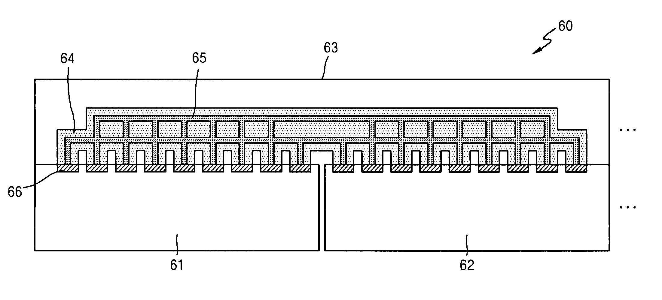
[0016] Example embodiments of the present invention relate to an interposer of a semiconductor device with a smaller dielectric constant.

[0017] Example embodiments of the present invention relate to an interposer of a semiconductor device having an air gap structure, a semiconductor device using the interposer, a multi-chip package using the interposer and methods of forming the interposer.

[0018] Example embodiments of the present invention provide an interposer of a semiconductor device with a decreased capacitance by reducing a dielectric constant of an interposer insulating layer.

[0019] Example embodiments of the present invention also provide a semiconductor device with an improved operation reaction speed by decreasing a capacitance using an interposer insulating layer.

[0020] Example embodiments of the present invention provide a multi-chip package with a faster operation reaction speed, requiring a smaller installation area.

[0021] According to an example embodiment of the...


PUM


Abstract

Example embodiments of the present invention relate to an interposer of a semiconductor device having an air gap structure, a semiconductor device using the interposer, a multi-chip package using the interposer and methods of forming the interposer. The interposer includes a semiconductor substrate including a void, a metal interconnect, provided within the void, thereby forming an air gap insulating the metal interconnect. The metal interconnect may be connected to a contact element, and may be maintained within the air gap using the contact element.

Description

PRIORITY STATEMENT [0001] This application claims the benefit of priority from Korean Patent Application No. 10-2005-0063761, filed on Jul. 14, 2005, in the Korean Intellectual Property Office, the disclosure of which is incorporated herein in its entirety by reference. BACKGROUND OF THE INVENTION [0002] 1. Field of the Invention [0003] Example embodiments of the present invention relate to an interposer of a semiconductor device having an air gap structure, a semiconductor device using the interposer, a multi-chip package using the interposer and methods of forming the interposer. [0004] 2. Description of the Related Art [0005] In semiconductor devices, unit elements such as a plurality of transistors, resistors and capacitors may be formed on a semiconductor substrate, and may be electrically connected to constitute a semiconductor integrated circuit. The unit elements constituting the semiconductor device may be connected to one another via interconnects. [0006] In the convention...

Claims


Application Information

Patent Timeline
IPC IPC(8): G01R31/02
CPCH01L23/535H01L25/0652H01L2224/48091H01L2224/48464H01L2924/1461H01L2924/00014H01L2924/00H01L23/498
Inventor KIM, CHANG-HYUNKIM, KYUNG-HO
Owner SAMSUNG ELECTRONICS CO LTD
Features
  • R&D
  • Intellectual Property
  • Life Sciences
  • Materials
  • Tech Scout
  • Unparalleled Data Quality
  • Higher Quality Content
  • 60% Fewer Hallucinations
Learn More