

Magnetoresistive element
a technology of magnetoresistor and element, applied in the field of magnetoresistive element, can solve the problem of not being able to satisfy both of them, and achieve the effect of satisfying both of them
- Summary
- Abstract
- Description
- Claims
- Application Information
AI Technical Summary
Benefits of technology
Problems solved by technology
Method used
Image

Examples
first embodiment
[1-1] First Embodiment
[0063]FIG. 4 is a schematic view showing an MTJ element according to the first embodiment of the present invention. The outline of the structure of the MTJ element according to the first embodiment will be described below.
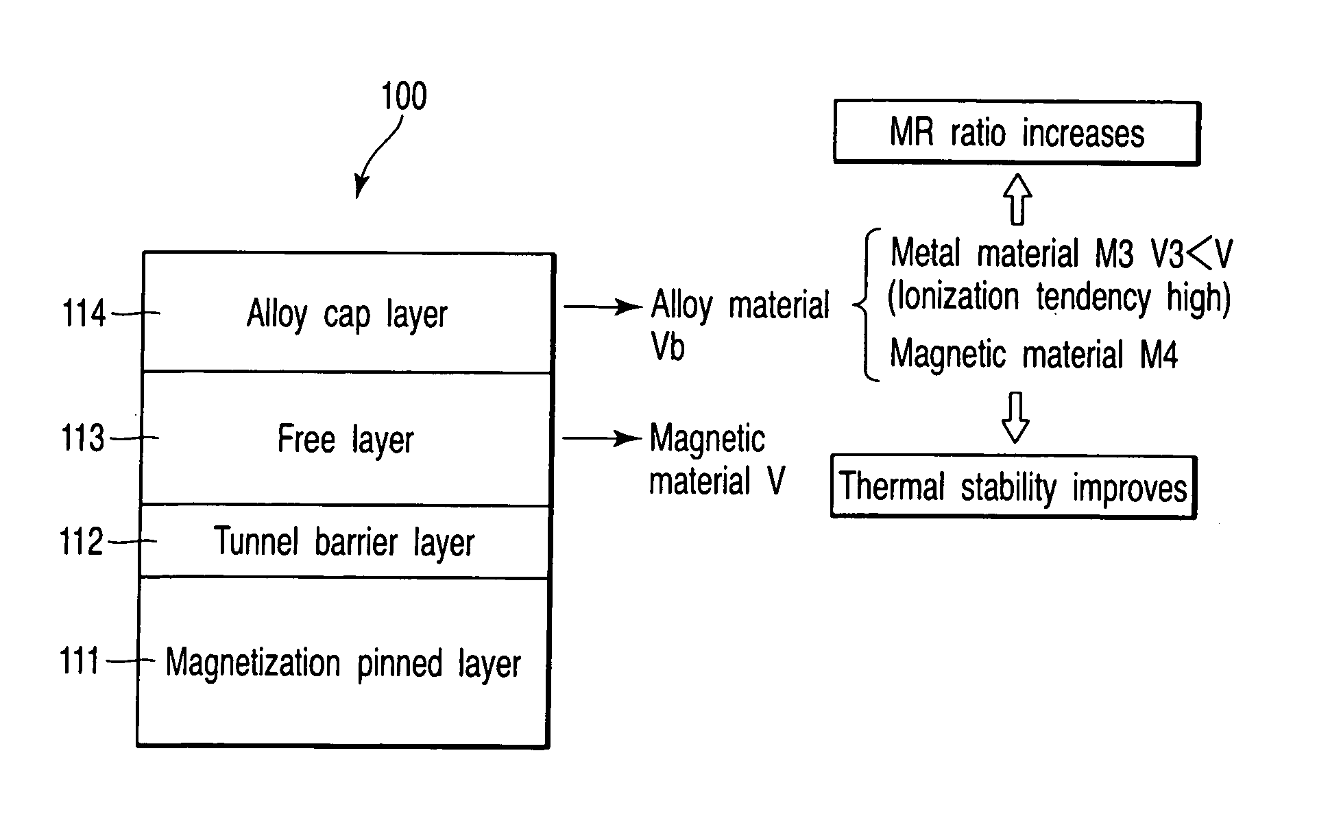
[0064] As shown in FIG. 4, an MTJ element 100 according to the first embodiment includes a magnetization pinned layer (magnetic layer) 111 whose magnetization is fixed, a free layer (magnetic layer) 113 whose magnetization reverses, a tunnel barrier layer (nonmagnetic layer) 112 sandwiched between the magnetization pinned layer 111 and the free layer 113, and an alloy cap layer 114 in contact with the free layer 113.
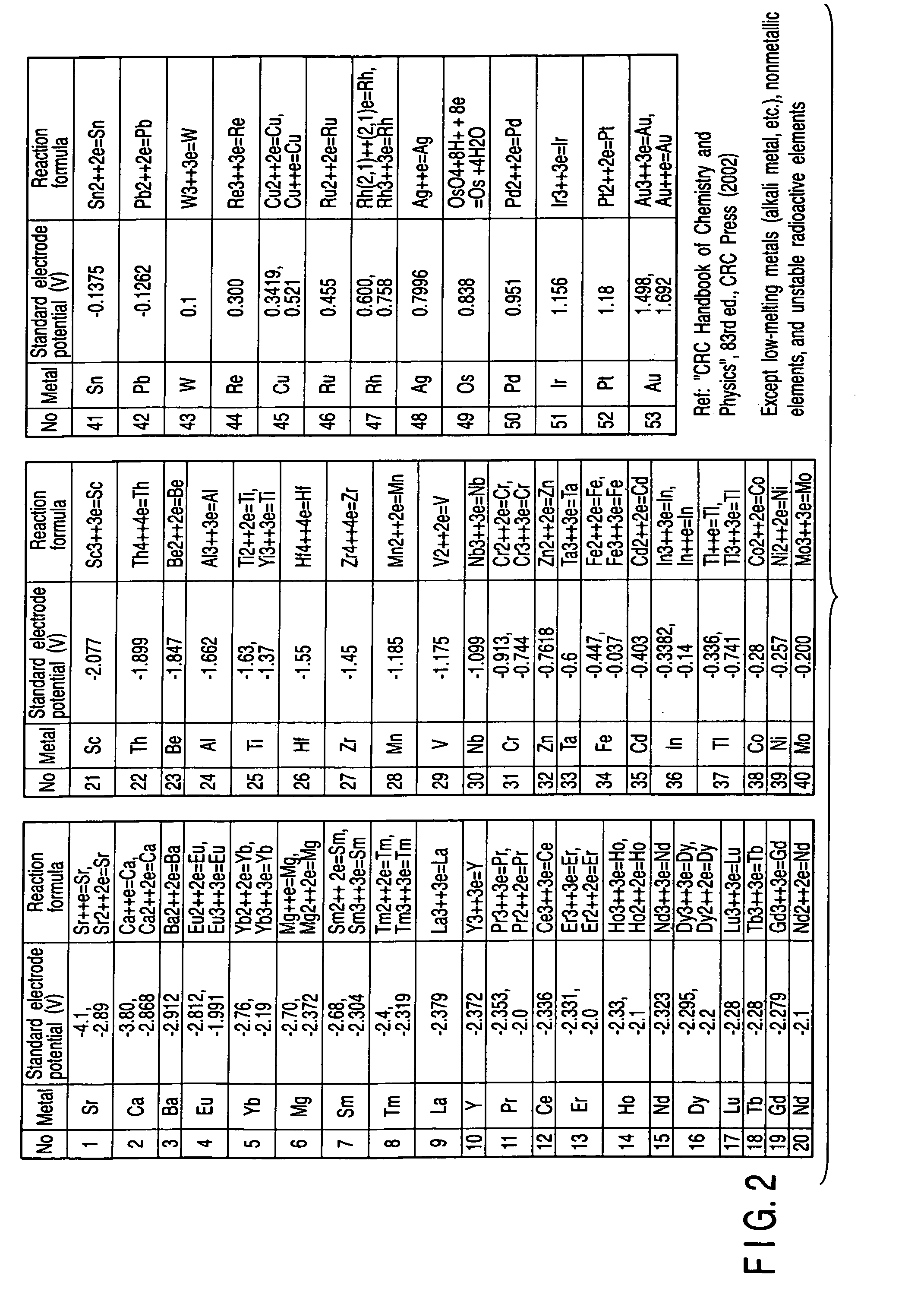
[0065] The alloy cap layer 114 is formed of a nonmagnetic layer. The alloy cap layer 114 is made of an alloy of a first metal material M1 and a second metal material M2. A standard electrode potential V1 of the first metal material M1 is lower than a standard electrode potential V of the free layer 113 adjacent to the alloy cap l...
example 1
[0100]FIG. 16 is a sectional view of an MTJ element according to Example 1 of the present invention. The structure of the MTJ element according to Example 1 will be described below.
[0101] As shown in FIG. 16, an MTJ element 100 according to Example 1 includes a lower interconnection connecting layer 121 made of Ta (thickness: 5 nm), a buffer layer 122 made of Ru (thickness: 1 nm), an antiferromagnetic layer 123 made of Pt—Mn (thickness: 15 nm), a magnetization pinned layer 111 made of Co—Fe (thickness: 5 nm), a tunnel barrier layer 112 made of aluminum oxide (AlOX) (thickness: 1 nm), a free layer 113 made of Ni—Fe (thickness: 4 nm), an alloy cap layer 114 made of an Ru—Ta alloy or Ru—Cr alloy (thickness: 3 nm), and a mask layer 124 made of Ta (thickness: 50 nm). The mask layer 124 functions as an etching mask, surface protection layer, and upper interconnection connecting layer.
example 2
[0102]FIG. 17 is a sectional view of an MTJ element according to Example 2 of the present invention. The structure of the MTJ element according to Example 2 will be described below.
[0103] As shown in FIG. 17, an MTJ element 100 according to Example 2 has a so-called synthetic ferrimagnetic pinned layer structure in which a magnetization pinned layer 111 includes a ferromagnetic layer 111a / nonmagnetic layer 111b / ferromagnetic layer 111c. The ferromagnetic layers 111a and 111c are antiferromagnetically coupled.
[0104] More specifically, the MTJ element 100 includes a lower interconnection connecting layer 121 made of Ta (thickness: 5 nm), an antiferromagnetic layer 123 made of Pt—Mn (thickness: 15 nm), the magnetic layer 111a made of Co—Fe (thickness: 2 nm), the nonmagnetic layer 111b made of an Ru—Ta alloy, the magnetic layer 111c made of Co—Fe (thickness: 2 nm), a tunnel barrier layer 112 made of aluminum oxide (AlOX) (thickness: 1 nm), a free layer 113 made of Ni—Fe (thickness: 4 ...
PUM
 Abstract
Description
Claims
Application Information