Method and apparatus for forming microstructures on polymeric substrates

a polymeric substrate and microstructure technology, applied in dough shaping, manufacturing tools, instruments, etc., can solve the problems of inability to achieve high-efficiency injection molding, etc., to achieve the effect of increasing the thickness of the stamper

Inactive Publication Date: 2007-01-18
ENERGY CONVERSION DEVICES INC
View PDF9 Cites 17 Cited by
  • Summary
  • Abstract
  • Description
  • Claims
  • Application Information

AI Technical Summary

Benefits of technology

[0017] In another aspect of the present invention there is provided a method of making a stamper for use in a continuous web forming process...

Problems solved by technology

Although injection-molding methods, such as those described above, can provide high quality optical memory disks with acceptable levels of birefringence and flatness, the rate of disk production is only in the neighborhood of several seconds.
Furthermore, present attempts to improve production rate by using various novel de-molding techniques or by using multi-cavity molds have had only limited success.
Besides lower than desired production rates, injection molding requires complex closed-loop control over numerous parameters.
It should also be noted that molding difficulty increases as the thickness of the replicated disk decreases.
Directly manufacturing these products via injection molding may not be practical.
These disturbances are associated with local turbulence, shear, and packing variation near the center gate in the mold and can produce locally poor flatness and high birefringence.
As the minimum track diameter is reduced, these problems may be exemplified.
This makes the overall system a highly complex process, at a point in the process where it may not be desirable.
Furthermore, because the disk manufacturer may not enjoy the same economies of scale that a plastic web manufacturer does, the cost per ...

Method used


Image

  • Method and apparatus for forming microstructures on polymeric substrates
  • Method and apparatus for forming microstructures on polymeric substrates
  • Method and apparatus for forming microstructures on polymeric substrates

Examples


Embodiment Construction

[0042] Reference is now made in more detail to the various aspects and several embodiments of the present invention(s).

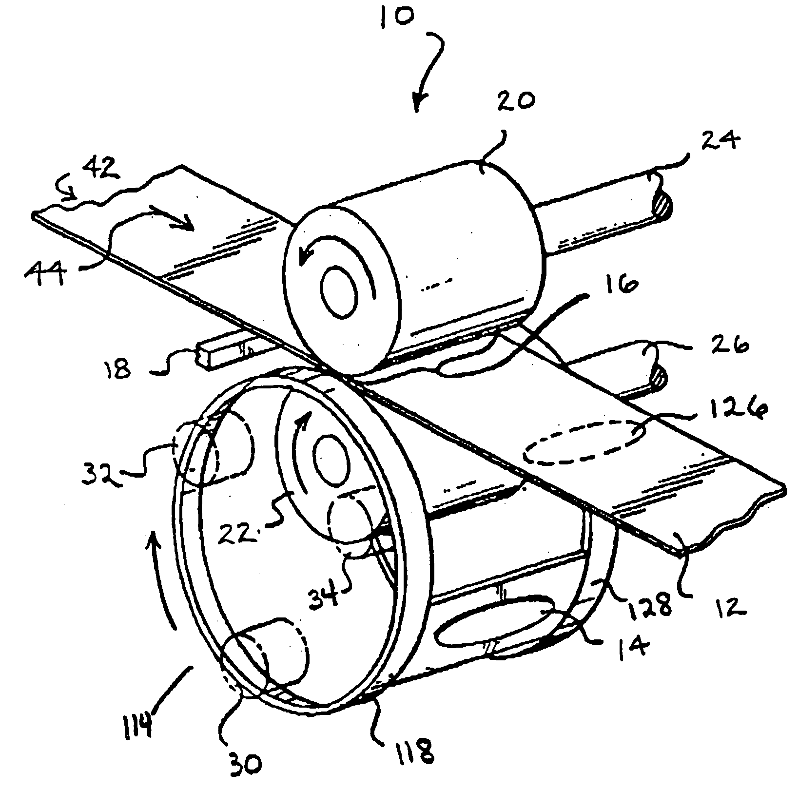
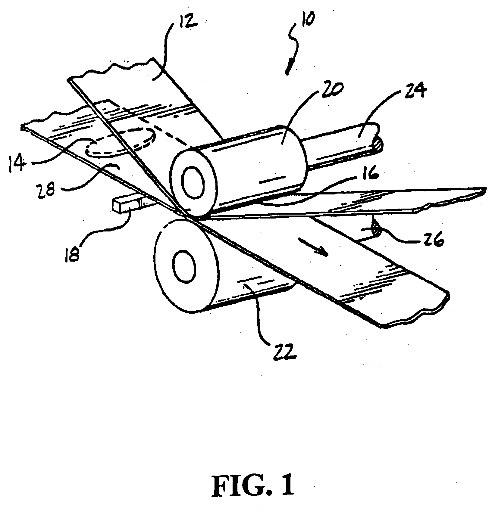
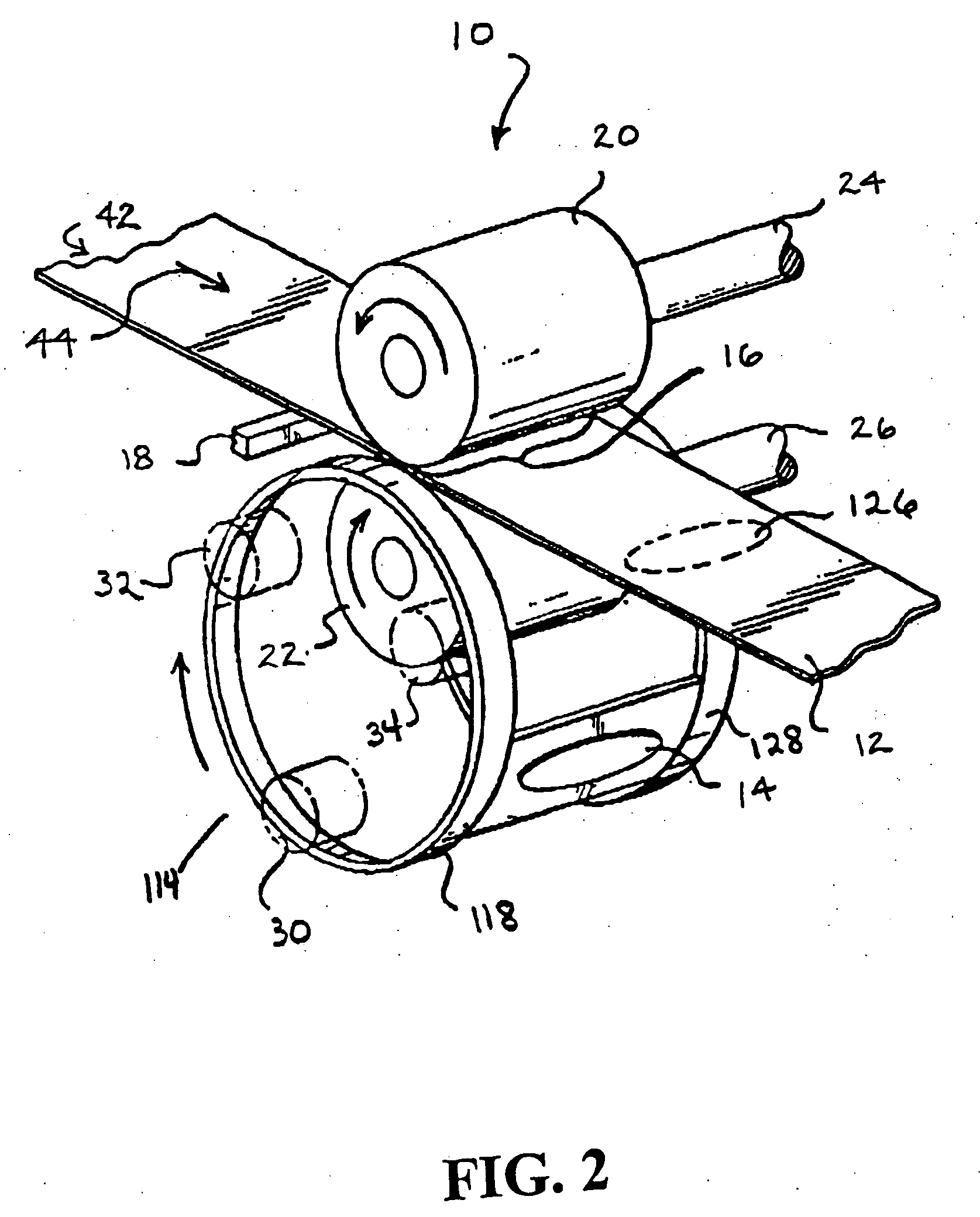
[0043] Referring now to FIG. 1, depicted therein is a device for forming optical memory in accordance with the present invention. The device includes a web payoff device, or simply a web payoff (not shown), a web path in which web material 12 travels, and a web forming apparatus disposed in the web path. The web forming apparatus 10 includes a stamper 14. The stamper carries a microstructure image for forming web. The stamper is carried by a support 28 and may be heated by any suitable heating device 18 and / or may also be heated by a drum or roller 22 in thermal contact with the stamper.

[0044] A pressure roller 20 and a backing roller 22 may be disposed in the web path to press the stamper into the surface of web material. The pressure roller and the backing roller form a nip zone 16. As shown, the nip zone 16 includes the narrowest region between the pressure rol...


PUM

PropertyMeasurementUnit
Thicknessaaaaaaaaaa
Thicknessaaaaaaaaaa
Thicknessaaaaaaaaaa

Abstract

An apparatus for forming microstructures in the surface of polymeric web materials for use as optical memory substrates. The microstructures may be formed by laminating a hot stamper to a web of material with a selective time/temperature profile. The stamper may be heated to melt flow the surface of the web and stabilize before separation. The stamper may be carried by a support that is independent of the press. The web of polymeric material may be provided with a flow enhancer to improve image formation. Also described herein are methods and apparatus for making optical memory modules, such as disks, which include novel stampers, coating applicators, and finishing systems.

Description

CROSS-REFERENCE TO RELATED APPLICATIONS [0001] The present invention relates to, and is entitled to the benefit of the earlier filing date and priority of, U.S. Provisional Patent Application No. 60 / 300997, filed Jun. 26, 2001, the disclosure of which is herein incorporated by reference.FIELD OF THE INVENTION [0002] The present invention relates generally to methods and apparatus for making optical memory. More particularly, the present invention pertains to forming substrates for optical memory and for making optical disks using continuous feed or roll-to-roll systems. BACKGROUND OF THE INVENTION [0003] Optical memory disks, such as CD (compact disks), CD-R, CD-RW; DVD (digital versatile disks), DVD-R, DVD-ROM, DVD-RAM, DVD+RW, DVD-RW, PD (phase change disks) and MO (magneto optical), etc., are typically manufactured by initially forming a substrate and then depositing one or more thin film layers upon the substrate. Substrates for optical memory are usually formed with a series of...

Claims


Application Information

Patent Timeline
IPC IPC(8): B29C43/46
CPCB29C43/00B29C43/222B29C59/04G11B7/263B29C2043/463B29C2059/023B29L2017/005B29C2043/025
Inventor HENNESSEY, MICHAELSTRAND, DAVIDCLARK, BARRYGASIOROWSKI, PAUL
Owner ENERGY CONVERSION DEVICES INC
Why Eureka
Try Eureka