
Atomic layer deposition of noble metal oxides

a technology of noble metal oxide and atomic layer, which is applied in the direction of chemical vapor deposition coating, metallic material coating process, coating, etc., can solve the problem of more or less self-saturation of reactions

Inactive Publication Date: 2007-01-18
ASM INTERNATIONAL
View PDF98 Cites 314 Cited by
  • Summary
  • Abstract
  • Description
  • Claims
  • Application Information

AI Technical Summary

Benefits of technology

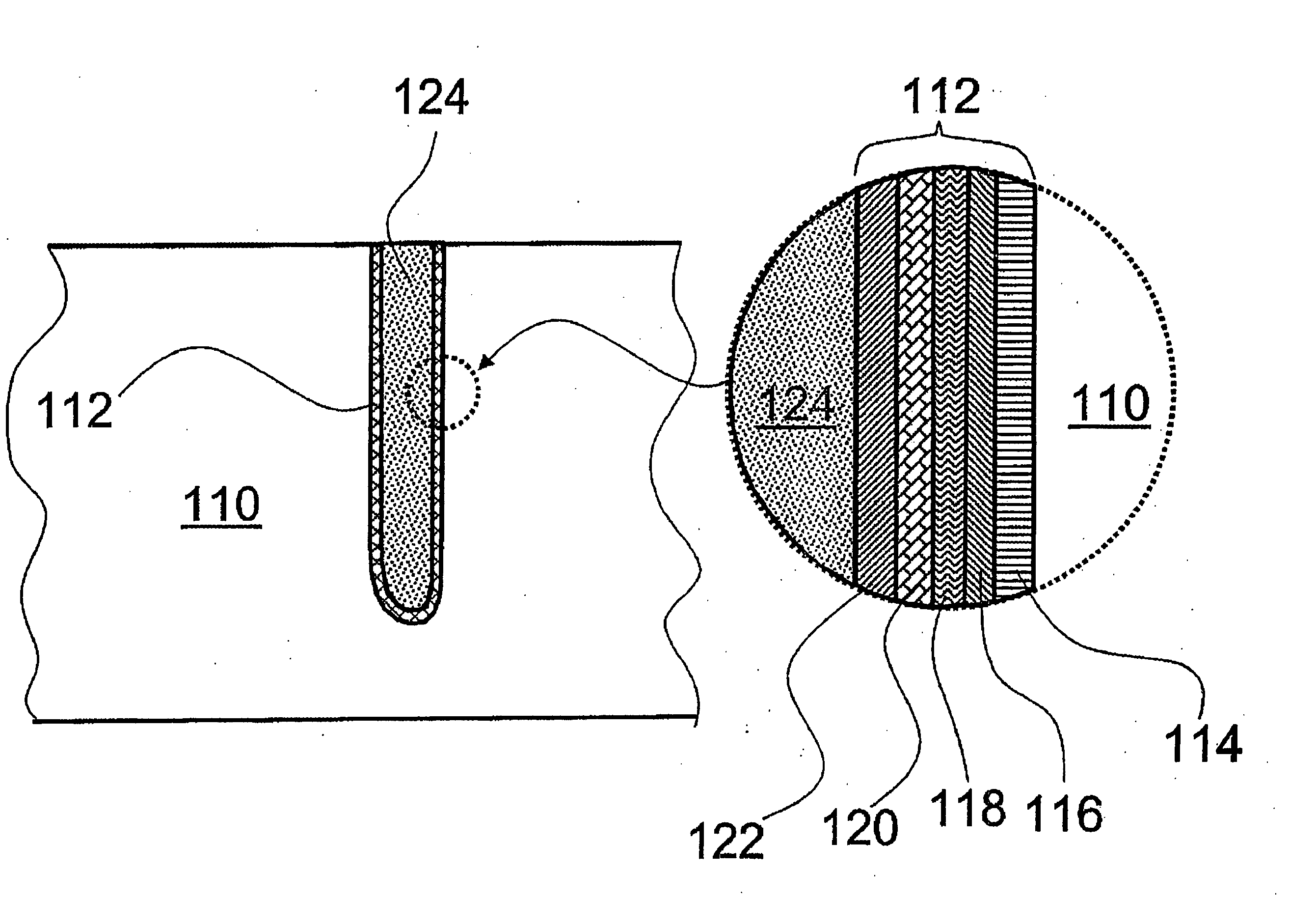
[0007] Thin films of conductive noble metal oxides, particularly Ru, Re, Os and Ir oxides, can be deposited using atomic layer deposition. A substrate is alternately contacted with a noble metal precursor and a second reactant comprising an oxygen source. In preferred embodiments the noble metal precursor is a betadiketonate compound and the oxygen source is ozone or oxygen plasma. The atomic layer deposition reaction is preferably carried out at a temperature of about 300° C. or less, more preferably at a temperature of about 200° C. or less.

Problems solved by technology

However, to provide for high conformality and thickness uniformity, these reactions are still more or less self-saturating.

Method used


Image

  • Atomic layer deposition of noble metal oxides
  • Atomic layer deposition of noble metal oxides
  • Atomic layer deposition of noble metal oxides

Examples


example 1

[0085] IrO2 was deposited by ALD on 5×5 cm2 soda glass and Si(111) substrates. The substrates were contacted with alternating pulses of Ir(acac)3 and ozone at a temperature of about 175° C.

[0086] The growth rate of the IrO2 film saturated at about 0.2 to about 0.3 Å / cycle with increasing ozone pulse time, as illustrated in FIG. 8. Similar results were obtained when the ozone dose was increased by adjusting the ozone needle valve (FIG. 9). XRD measurements revealed that the as-deposited IrO2 films were amorphous with an identifiable crystalline IrO2 phase (FIG. 10). Resistivities were about 250 μΩ·cm. The films were dark gray and semitransparent on the soda lime glass substrates and bronze tinted on the silicon substrates.

[0087] RhO2 films were grown on 5×5 cm soda glass and Si(111) substrates by contacting them with alternating pulses of Rh(acac)3 and ozone at a temperature of about 175° C. to about 200° C. The films were grayish and semitransparent in color and partly reflective....


PUM

PropertyMeasurementUnit
temperatureaaaaaaaaaa
timeaaaaaaaaaa

Abstract

Electrically conductive noble metal oxide films can be deposited by atomic layer deposition (ALD)-type processes. In preferred embodiments, Re, Ru, Os and Ir oxides are deposited by alternately and sequentially contacting a substrate with vapor phase pulses of a noble metal precursor and an oxygen source. The noble metal precursor is preferably a betadiketonate compound and the oxygen source is preferably ozone or oxygen plasma. The deposition temperature may be less than about 200° C.

Description

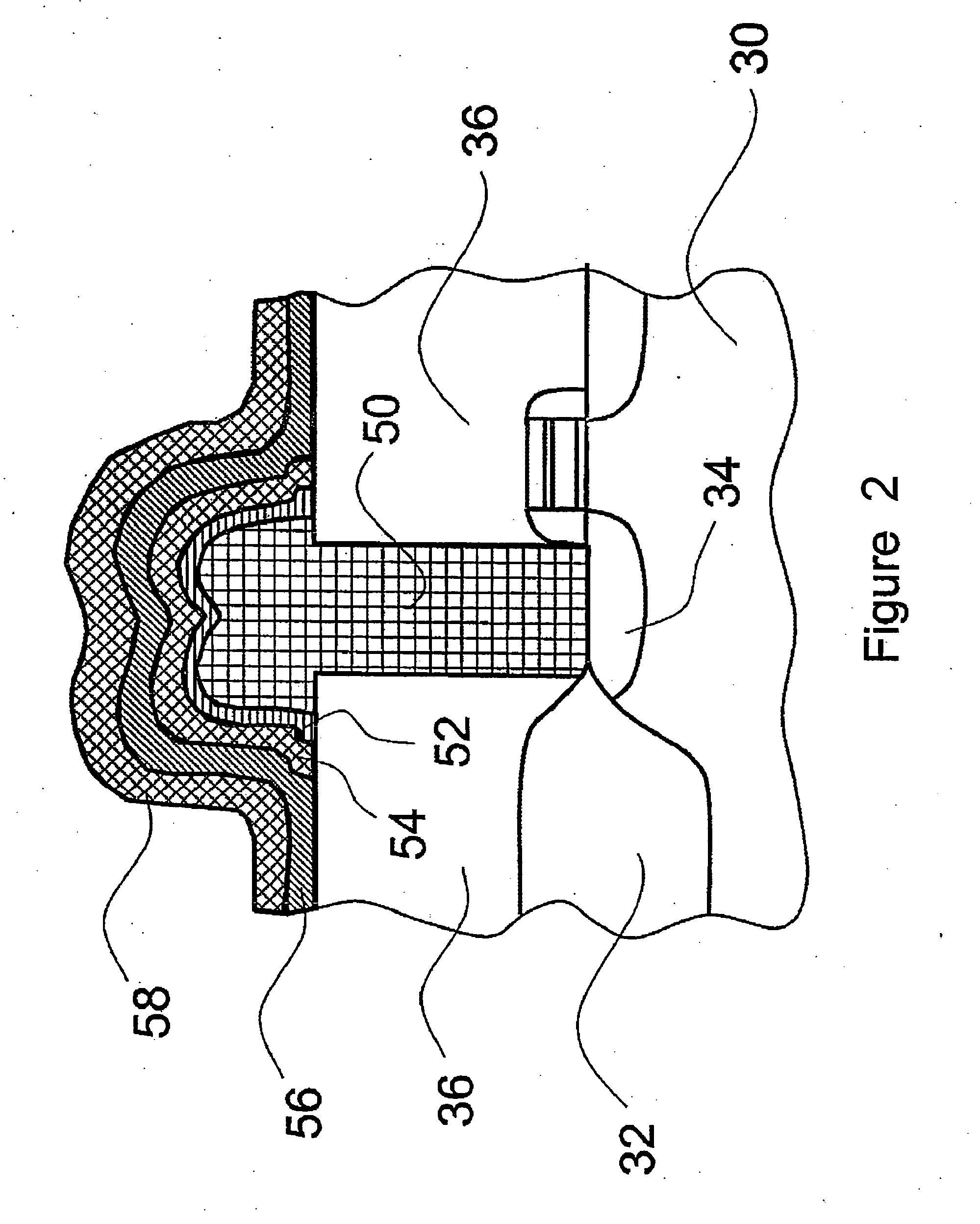
BACKGROUND OF THE INVENTION [0001] 1. Field of the Invention [0002] The present invention relates generally to processes for producing noble metal oxide thin films on a substrate by atomic layer deposition. [0003] 2. Description of the Related Art [0004] Noble metal oxide thin films have high work function, good oxidation resistance and good barrier properties. As a result, they have a variety of potential applications in microelectronics and in other fields. For example, in the semiconductor industry noble metal oxides can be used as a material for electrodes in DRAMs and FRAMs, as gate electrodes in integrated circuits and as barrier and seed layers for interconnect metallization. [0005] ALD is a self-limiting process, whereby alternated pulses of reaction precursors saturate a substrate surface and leave no more than one monolayer of material per pulse. The deposition conditions and precursors are selected to ensure self-saturating reactions, such that an adsorbed layer in one pu...

Claims


Application Information

Patent Timeline
Patent Type & Authority Applications(United States)
IPC IPC(8): C23C16/00
CPCC23C16/45525C23C16/40
Inventor HAMALAINEN, JANIRITALA, MIKKOLESKELA, MARKKU
Owner ASM INTERNATIONAL
Learn More