
Methods and systems for characterizing semiconductor materials

a semiconductor material and optical technique technology, applied in semiconductor/solid-state device testing/measurement, instruments, digital computer details, etc., can solve the problem of not readily apparent two individual critical points, and achieve the effect of reducing or substantially eliminating errors due to correlation, curve fitting, and the like of conventional in-line optical techniques

Inactive Publication Date: 2007-01-18
SEMATECH
View PDF12 Cites 5 Cited by
  • Summary
  • Abstract
  • Description
  • Claims
  • Application Information

AI Technical Summary

Benefits of technology

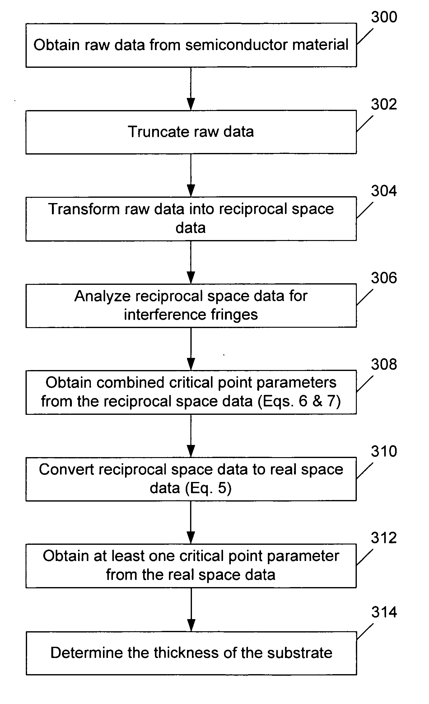
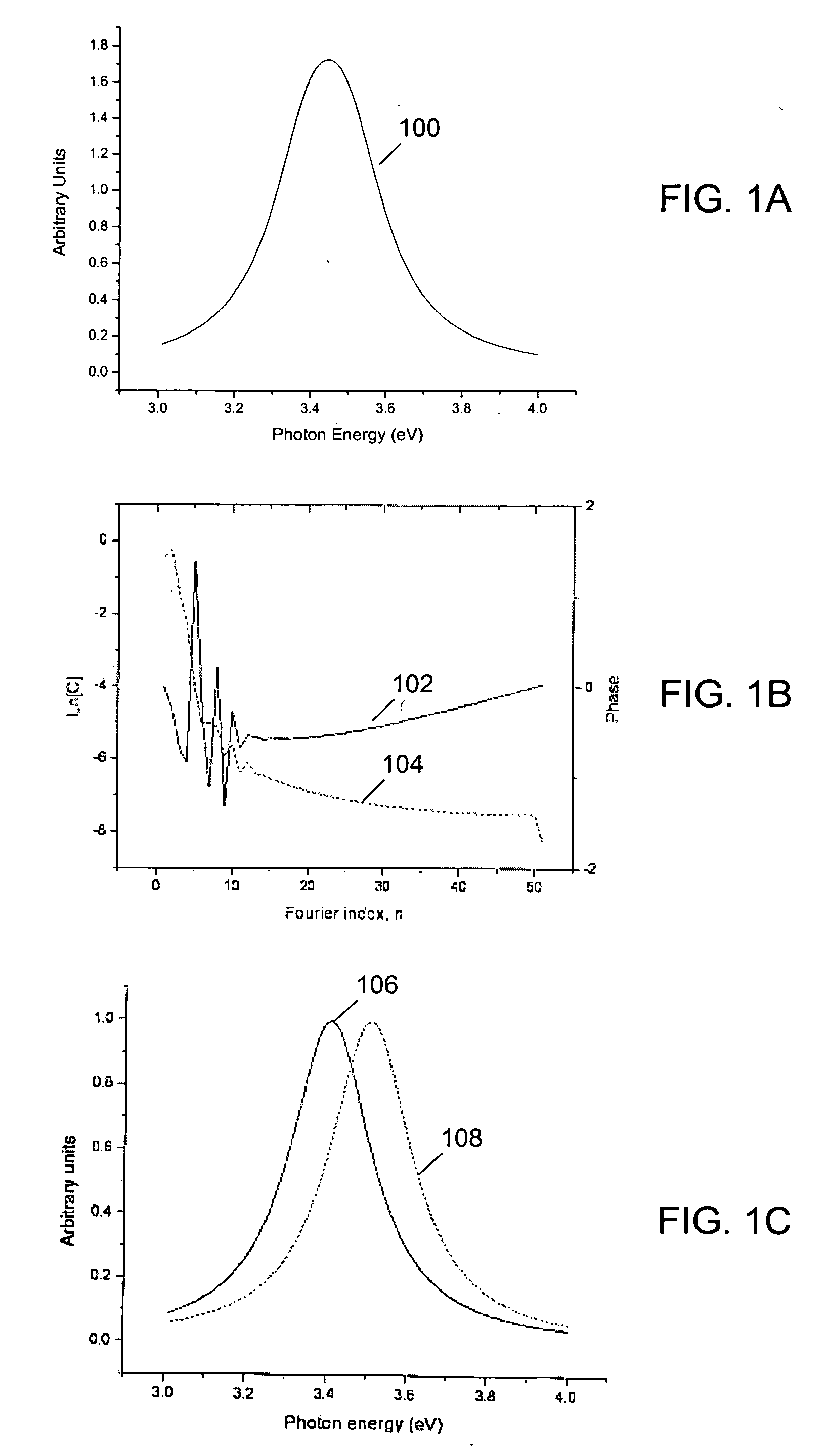
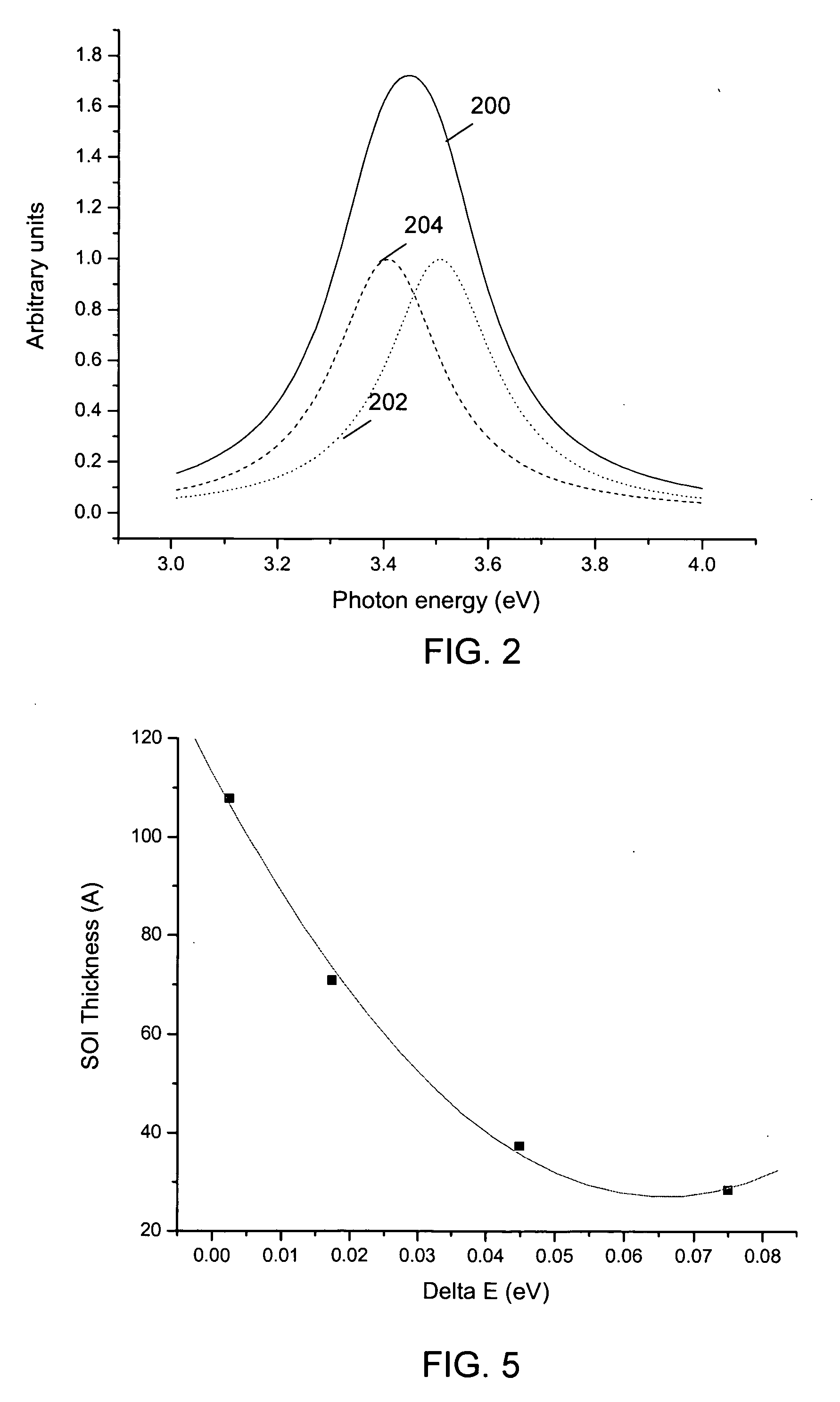
[0009] In one respect, data that contains contributions from two different critical points, one bulk 3D silicon and one from a 2D confined silicon layer may be analyzed for SOI substrates. Alternatively, for substrates such as, but not limited to, sSOI or sGeOI, a 3D critical point and a critical point due to a strained silicon layer may be analyzed. However, when viewed in real space (i.e., as a function of photon energy or wavelength), the two individual critical points are not readily apparent. As such, in one embodiment, this data may be mapped into reciprocal space (i.e., as a function of Fourier coefficient index, n), such that the information from the critical points is separated from that of the baseline effects due to internal reflections and noise. Once the critical point parameters are realized in reciprocal space, they then can be re-cast in real space independent of baseline information and film interference effects that initially convolute the signal as governed by the Fresnel equations. Identification of the separate inversion origins of each critical point (band gap) may then be used to calculate the thickness of the quantum confined layer. In one embodiment, the techniques used do not require curve fitting or linear regression techniques. As such, errors due to correlation, curve fitting, and the like of conventional in-line optical techniques may be reduced or substantially eliminated.

Problems solved by technology

However, when viewed in real space (i.e., as a function of photon energy or wavelength), the two individual critical points are not readily apparent.

Method used


Image

  • Methods and systems for characterizing semiconductor materials
  • Methods and systems for characterizing semiconductor materials
  • Methods and systems for characterizing semiconductor materials

Examples


Embodiment Construction

[0024] The disclosure and the various features and advantageous details are explained more fully with reference to the nonlimiting embodiments that are illustrated in the accompanying drawings and detailed in the following description. Descriptions of well known starting materials, processing techniques, components, and equipment are omitted so as not to unnecessarily obscure the invention in detail. It should be understood, however, that the detailed description and the specific examples, while indicating embodiments of the invention, are given by way of illustration only and not by way of limitation. Various substitutions, modifications, additions, and / or rearrangements within the spirit and / or scope of the underlying inventive concept will become apparent to those skilled in the art from this disclosure.

[0025] The disclosure provides for characterizing quantum mechanical properties seen in semiconductor materials, particularly thin substrates (having about or less than approxima...


PUM


Abstract

Methods for determining parameters of a semiconductor material, for example, non-classical substrates such as silicon-on-insulator (SOI) substrates, strained silicon-on-insulator (sSOI) substrates, silicon-germanium-on-insulator (GeOI) substrates, and strained silicon-germanium-on-insulator (sGeOI) substrates are described. The method provides steps for transforming data corresponding to the semiconductor material from real space to reciprocal space. The critical points are isolated in the reciprocal state and corresponding critical energies of the critical points are determined. The difference between the critical energies may be used to determine a thickness of a layer of the semiconductor material, in particular, a quantum confined layer.

Description

[0001] This application is a continuation-in-part of, claims priority to, and incorporates by reference, co-pending patent application Ser. No. 11 / 179,357 entitled “METHODS AND SYSTEMS FOR CHARACTERIZING SEMICONDUCTOR MATERIALS” which was filed on Jul. 12, 2005.BACKGROUND OF THE INVENTION [0002] 1. Field of the Invention [0003] The present invention relates generally to optical techniques for characterizing semiconductor materials. More particularly, the present invention involves methods for determining parameters in non-classical semiconductor materials including, without limitation, silicon-on-insulator (SOI) substrates, strained silicon-on-insulator (sSOI) substrates, silicon-germanium-on-insulator (GeOI) substrates, and strained silicon-germanium-on-insulator (sGeOI) substrates. [0004] 2. Description of Related Art [0005] Current integrated circuit (IC) manufacturing processes employ bulk silicon substrates for the fabrication of semiconductor devices. During the manufacturing ...

Claims


Application Information

Patent Timeline
IPC IPC(8): H01L21/66G01R31/26
CPCG01B11/0616
Inventor PRICE, JAMES MARTIN
Owner SEMATECH
Learn More