Transmit and receive interface array for highly integrated ultrasound scanner

a technology of ultrasound scanner and interface array, which is applied in the field of integrated circuitry, can solve the problems of inability to connect several thousand elements to respective pulsers in the system, inability to achieve ergonomics, and large amount of power, and achieves the effect of small footprint and minimal power expenditur

Inactive Publication Date: 2007-01-18
GENERAL ELECTRIC CO
View PDF5 Cites 101 Cited by
  • Summary
  • Abstract
  • Description
  • Claims
  • Application Information

AI Technical Summary

Benefits of technology

[0014] There is a need to solve the problem of driving a large number of small ultrasound transducers in a two-dimensional array configuration with minimal power expenditure and in a small footprint.
[0015] The invention is directed to an ultrasonic transducer probe having a highly integrated interface circuit array. Low-voltage transmit control signals from the system are transmitted on the system transmit channels via the ultrasound probe cable and into the interface circuit array. These transmit control signals are routed through the interface circuit array using a dense switching matrix. Once the low-voltage transmit control signals reach individual cells within the interface array, they are decoded and used to control local high-voltage pulser circuits to drive individual ultrasound transducer elements made up of selected subelements that are co-integrated with the interface electronics. The interface cell circuitry further comprises a high-voltage transmit/receive switch, which is closed when the high-voltage pulser is transmitting to protect the low-voltage components.
[0016] One aspect of the invention is a device comprising a multiplicity of ultrasonic transducers and a multiplicity of interface circuit cells, each of the ultrasonic transducers being electrically coupled to a respective one of the interface circuit cells, and each of the interface circuit cells comprising a high-voltage pulser for driving a respective ultrasonic transducer, a low-voltage switch for providing pulser control signals when the low-voltage switch is on, a low-voltage digital control circuit that outputs switch state control signals for controlling the state of the low-voltage switch, and a high-voltage transmit/receive switch disposed between the low-voltage switch and the respective ultrasonic transducer for providing a path for receive signals from the respective ultrasonic transducer to the low-voltage switch when the transmit/receive switch is on, wherein the transmit/receive switch blocks the pulser output from reaching the low-voltage switch via the path when the transmit/receive switch is off.
[0017] Another aspect of the invention is a probe comprising: a multiplicity of ultrasonic transducers; a multiplicity of high-voltage pulsers coupled for respectively driving the transducers in accordance with low-voltage pulser control signals inputted to the probe in a transmit mode; and a multiplicity of high-voltage transmit/receive switches, each of the high-voltage transmit/receive switches having an input electrically connected to a junction at an electrical connection between a respectiv

Problems solved by technology

These systems typically are able to drive only about 128-256 channels and consume a large amount of power.
Connecting several thousand elements to respective pulsers in the system is technically not feasible because a cable bundle of coaxial or other wire comprising a sufficient number of conductors for several thousand elements would be too thick and heavy to be ergonomically viable.
Also, a cable that would connect the system pulsers to the transducer elements would present a very large capacitance load compared to the impedance of the two-dimensional ar

Method used


Image

  • Transmit and receive interface array for highly integrated ultrasound scanner
  • Transmit and receive interface array for highly integrated ultrasound scanner
  • Transmit and receive interface array for highly integrated ultrasound scanner

Examples


Embodiment Construction

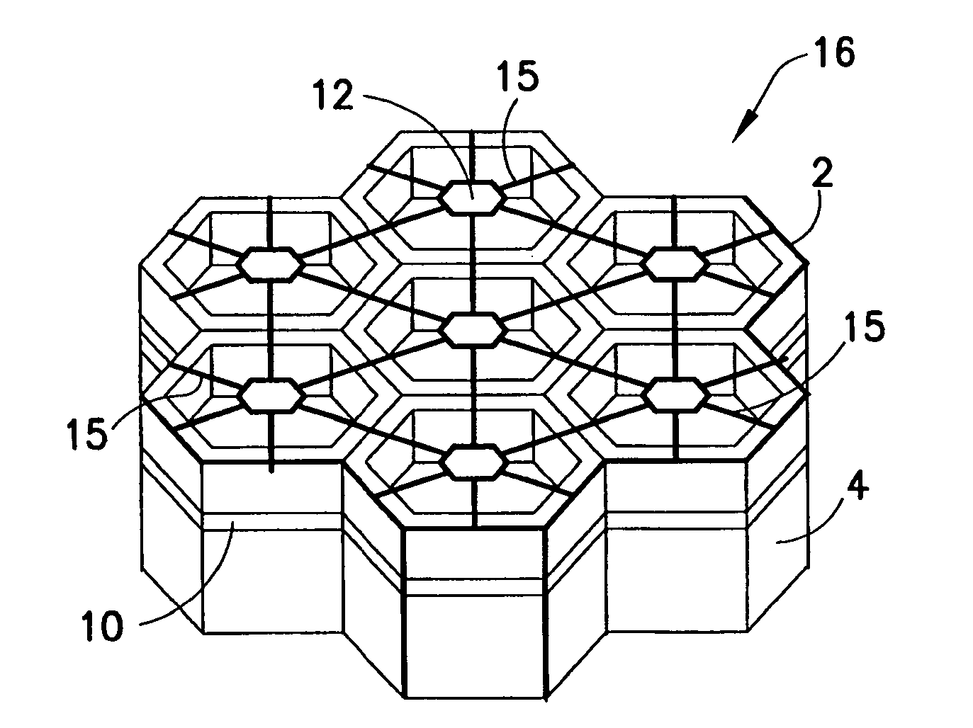
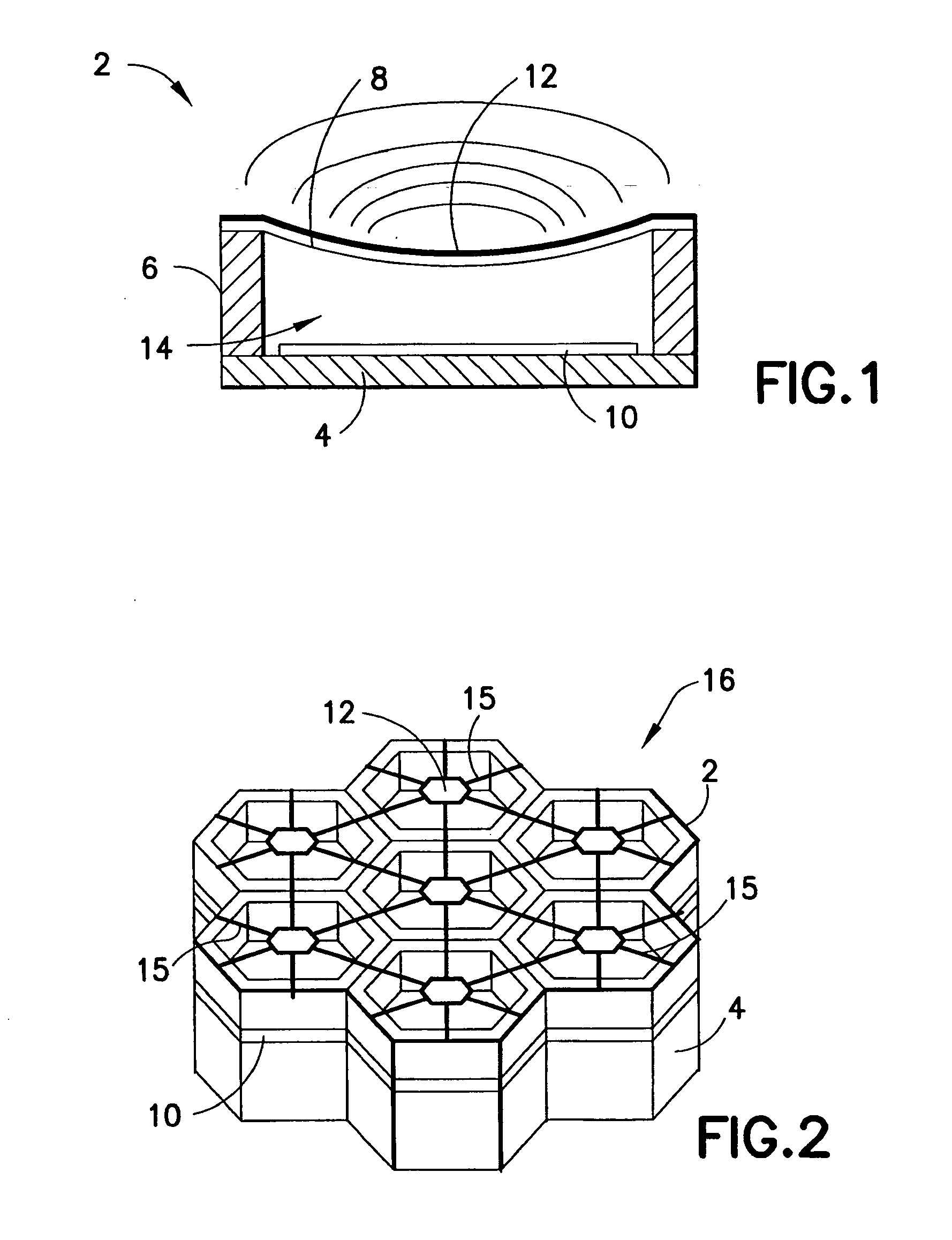
[0048] Recently semiconductor processes have been used to manufacture ultrasonic transducers of a type known as micromachined ultrasonic transducers (MUTs), which may be of the capacitive (cMUT) or piezoelectric (PMUT) variety. MUTs are tiny diaphragm-like devices with electrodes that convert the sound vibration of a received ultrasound signal into a modulated capacitance. For transmission the capacitive charge is modulated to vibrate the diaphragm of the device and thereby transmit a sound wave. One advantage of MUTs is that they can be made using semiconductor fabrication processes, such as microfabrication processes grouped under the heading “micromachining”. The systems resulting from such micromachining processes are typically referred to as “micromachined electro-mechanical systems” (MEMS). As explained in U.S. Pat. No. 6,359,367: [0049] Micromachining is the formation of microscopic structures using a combination or subset of (A) Patterning tools (generally lithography such a...


PUM


Abstract

An ultrasonic transducer probe having a highly integrated interface circuit array. Low-voltage transmit control signals from the system are transmitted on the system transmit channels via the ultrasound probe cable and into the interface circuit array. These transmit control signals are routed through the interface circuit array using a dense switching matrix. Once the low-voltage transmit control signals reach individual cells within the interface array, they are decoded and used to control local high-voltage pulser circuits to drive individual ultrasound transducer elements made up of selected subelements that are co-integrated with the interface electronics. The interface cell circuitry further comprises a high-voltage transmit/receive switch, which is closed when the high-voltage pulser is transmitting to protect the low-voltage components.

Description

STATEMENT REGARDING FEDERALLY SPONSORED RESEARCH AND DEVELOPMENT [0001] The United States Government may have certain rights in this invention pursuant to U.S. Government Contract Number 1R01 EB002485 awarded by the National Institutes of Health.BACKGROUND OF THE INVENTION [0002] This invention generally relates to integrated circuitry for use in conjunction with ultrasonic transducer elements. In particular, the invention relates to integrated low-voltage and high-voltage circuitry to be located in the probe handle in an ultrasound imaging system. One specific application for such transmit / receive switches is in medical diagnostic ultrasound imaging systems. Another specific example is for non-destructive evaluation of materials, such as castings, forgings, or pipelines. [0003] For the purposes of this disclosure, “low voltage” means any voltage level that is readily implemented in widely available “standard” semiconductor processes. This could be anywhere from 2.5 to 5 V (for CMOS...

Claims


Application Information

Patent Timeline
IPC IPC(8): A61B8/00
CPCG01S7/5208A61B8/56G10K11/341
Inventor THOMENIUS, KAI E.WODNICKI, ROBERT GIDEONLI, YE-MING
Owner GENERAL ELECTRIC CO
Why Eureka
Try Eureka