Photoresist stripper composition and methods for forming wire structures and for fabricating thin film transistor substrate using composition

a technology of composition and stripper, applied in the field of photoresist stripper composition, can solve the problems of affecting the performance of thin film transistor substrates, and overcoming significant signal delays, so as to prevent oxidation and corrosion of wire structures and good stripping capability

Active Publication Date: 2007-01-25
SAMSUNG DISPLAY CO LTD
View PDF0 Cites 28 Cited by
  • Summary
  • Abstract
  • Description
  • Claims
  • Application Information

AI Technical Summary

Benefits of technology

[0008] The present invention provides embodiments of a photoresist stripper composition; a method for forming wire structure using the photoresist stripper composition embodiments; and a method for fabricating a thin film transistor substrate using the photoresist stripper composition embodiments. The inventive photoresist stripper composition embodiments according to the present invention exhibit good stripping capability, while substantially preventing the oxidation and corrosion of wire structures, including copper wire structures. According to an aspect of the present invention, a photoresist stripper composition is provided, having butyl diglycol in a concentration of between about 50 weight percent concentration (WT %) to about 70 WT %; an alkylpyrrolidone of between about 20 WT % to about 40 WT %; an organic amine compound in a concentration of between about 1 WT % to about 10 WT %; aminopropylmorpholine in a concentration of between about 1 WT % to about 5 WT %, and a mercapto compound in a concentration of between about 0.01 WT % to about 0.5 WT %.

Problems solved by technology

However, CRTs bear the disadvantages of being heavier, bulkier, and more power-hungry than flat panel displays with a comparable display size.
Larger screen displays using fine-patterned TFTs face the challenge of overcoming significant signal delays due to longer signal lines with reduced cross-sectional areas.
However, copper may adhere poorly to an underlying structure, and thus, may be susceptible to separating or peeling off from the underlying structure.
Furthermore, even if made to adhere to underlying structures, copper can be susceptible to by oxidation or corrosion by the photoresist stripper materials used to remove photoresist films during the patterning process.
Copper degradation reduces the advantages of the copper conductive layer as a low-resistivity wire structure, because it increases the total resistance of the wire structures.
However, these techniques may reduce the reliability of copper wiring, because they tend to reduce the stripping capability of a photoresist stripper and allow the formation of a residual photoresist film.

Method used


Image

  • Photoresist stripper composition and methods for forming wire structures and for fabricating thin film transistor substrate using composition
  • Photoresist stripper composition and methods for forming wire structures and for fabricating thin film transistor substrate using composition
  • Photoresist stripper composition and methods for forming wire structures and for fabricating thin film transistor substrate using composition

Examples


Embodiment Construction

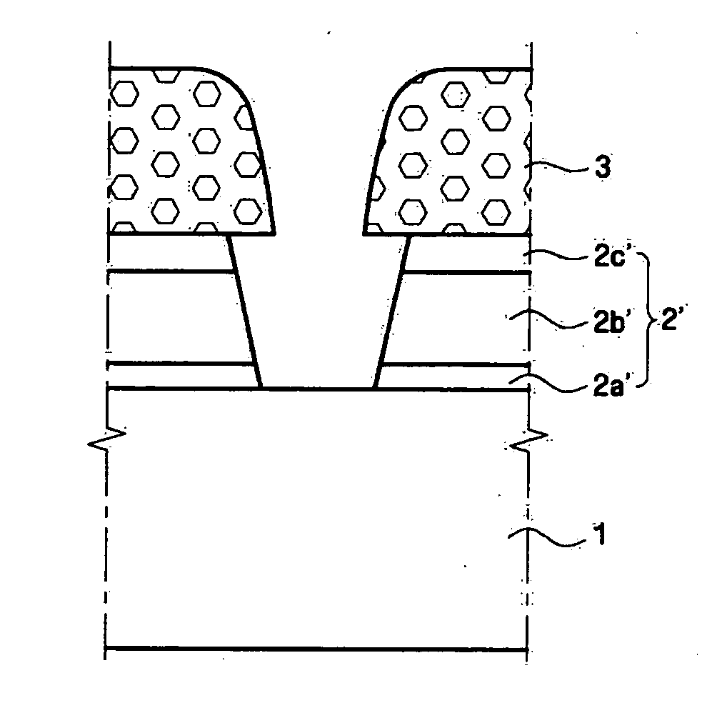
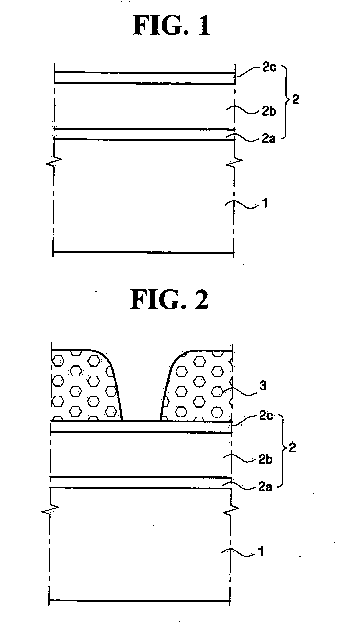
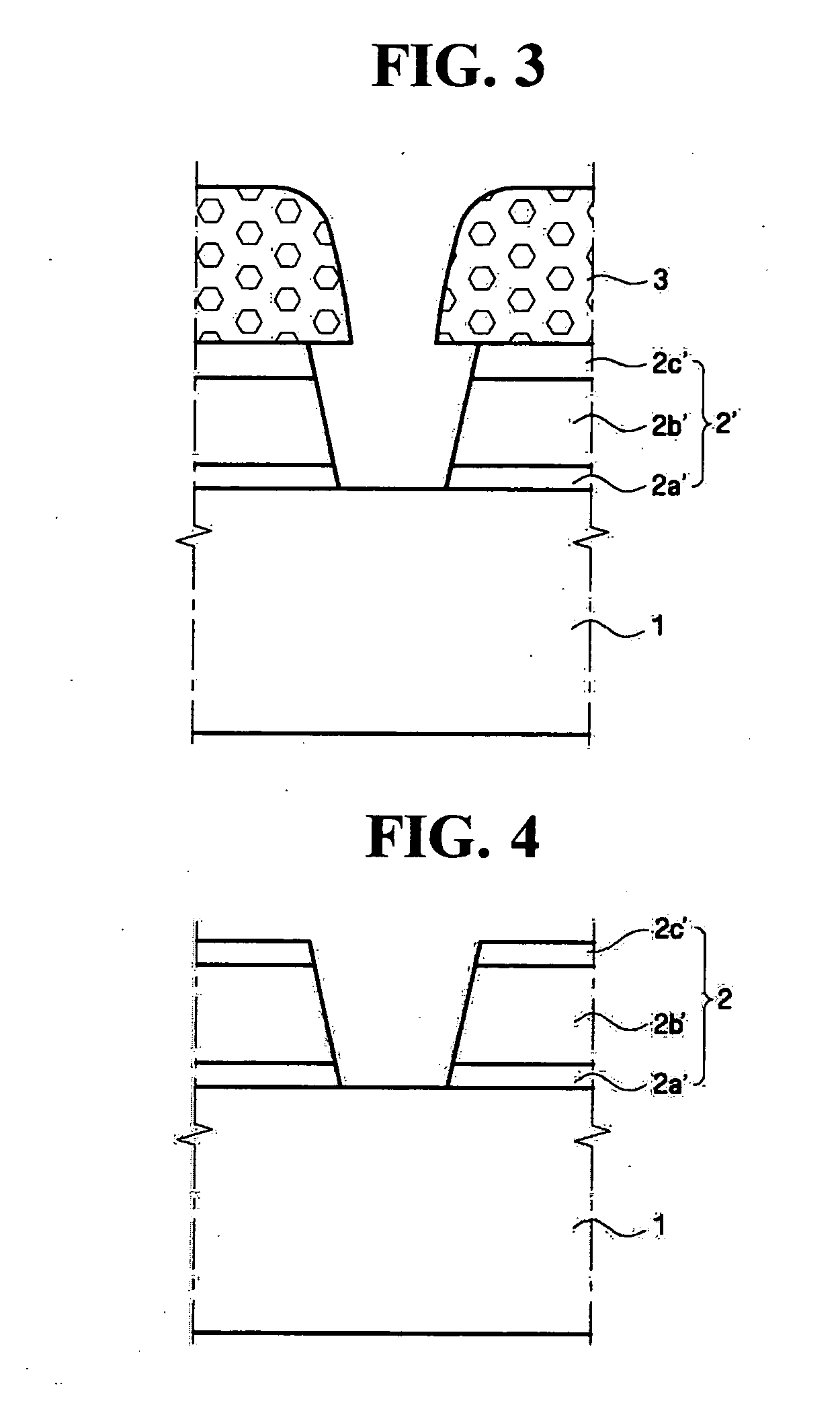
[0027] The present invention will now be described more fully hereinafter with reference to the accompanying drawings, in which the same reference numbers indicate the same components throughout the specification. In the attached figures, the thickness of layers and regions may be exaggerated for clarity. It will also be understood that when a layer is referred to as being “on” another layer or substrate, it can be directly on the other layer or substrate, or intervening layers may also be present. In contrast, when an element is referred to as being “directly on” another element, there are no intervening elements present. A method for forming a wire structure according to an embodiment of the present invention will now be described more fully with reference to the accompanying drawings, in which FIGS. 1 through 3 are sequential sectional views illustrating a wire structure forming method according to an embodiment of the present invention. Referring to FIG. 1, lower structure 1 is ...


PUM

PropertyMeasurementUnit
temperatureaaaaaaaaaa
contact timeaaaaaaaaaa

Abstract

A photoresist stripper composition, a method for forming wire structures thereby, and a method of fabricating a thin film transistor substrate using the composition. The photoresist stripper composition includes about 50 WT % to about 70 WT % of butyldiglycol, about 20 to about 40 WT % of an alkylpyrrolidone, about 1 WT % to about 10 WT % of an organic amine compound, about 1 to about 5 WT % of aminopropylmorpholine, and about 0.01 to about 0.5 WT % of a mercapto compound.

Description

[0001] This application claims priority from Korean Patent Application No. 10-2005-0067479 filed on Jul. 25, 2005 in the Korean Intellectual Property Office, the disclosure of which is incorporated herein by reference in its entirety. BACKGROUND OF THE INVENTION [0002] 1. Field of the Invention [0003] The present invention relates to a photoresist stripper composition, and more particularly, to a photoresist stripper composition for forming copper wire structures, a method for forming copper wire structures using the composition, and a method for fabricating a thin film transistor substrate using the composition. [0004] 2. Description of the Related Art [0005] Semiconductor integrated circuits, devices, and apparatus play an increasing important role in modern society, and are widely used in many industries. In particular, a growing information-oriented society continually drives the development of new electronic displays, with new display functions being devised and added to meet t...

Claims


Application Information

Patent Timeline
Patent Type & Authority Applications(United States)
IPC IPC(8): H01L21/44
CPCG03F7/425H01L21/2855H01L21/31133H01L21/76838H01L27/1288H01L29/41733H01L29/458H01L29/4908H01L27/124H01L21/7685G03F7/42G03F7/00H01L21/28
Inventor PARK, HONG-SICKKIM, SHI-YULCHOUNG, JONG-HYUNSHIN, WON-SUK
Owner SAMSUNG DISPLAY CO LTD
Why Eureka
Try Eureka