Eureka AIR delivers breakthrough ideas for toughest innovation challenges, trusted by R&D personnel around the world.

Prevention of trench photoresist scum

a technology of photoresist scum and trenches, which is applied in the direction of semiconductor/solid-state device manufacturing, basic electric elements, electric devices, etc., can solve the problems of difficult patterning of vias, increased manufacturing costs, and formation of photoresist scum on the sidewalls and bottom surfaces of via trenches, so as to prevent the formation of photoresist scum, reduce manufacturing costs, and improve manufacturing yields and device performance

Inactive Publication Date: 2007-01-25
TAIWAN SEMICON MFG CO LTD
View PDF6 Cites 10 Cited by
  • Summary
  • Abstract
  • Description
  • Claims
  • Application Information

AI Technical Summary

Benefits of technology

[0012] Advantages of embodiments of the present invention include preventing the formation of photoresist scum in semiconductor device patterning processes. Manufacturing yields and device performance are improved, and the cost of manufacturing is decreased, by the use of embodiments of the present invention. The required queue time required for processing steps to manufacture the semiconductor devices is decreased; thus, the queue time may be increased without the formation of photoresist scum.

Problems solved by technology

Vias can be challenging to pattern, because they typically are quite small, and may comprise a minimum feature size of a semiconductor device in some applications, for example.
As feature sizes become smaller and smaller, as is the trend in the semiconductor industry, via formation becomes even more challenging.
A problem in prior art methods of etching via patterns in dielectric materials is the formation of photoresist scum on the sidewalls and the bottom surfaces of the via trenches being formed.
Lengthy cleaning processes may be required in an attempt to remove the photoresist scum from within the via trenches.
Photoresist scum increases the cost of manufacturing and may decrease product yields.

Method used


Image

  • Prevention of trench photoresist scum
  • Prevention of trench photoresist scum
  • Prevention of trench photoresist scum

Examples


Embodiment Construction

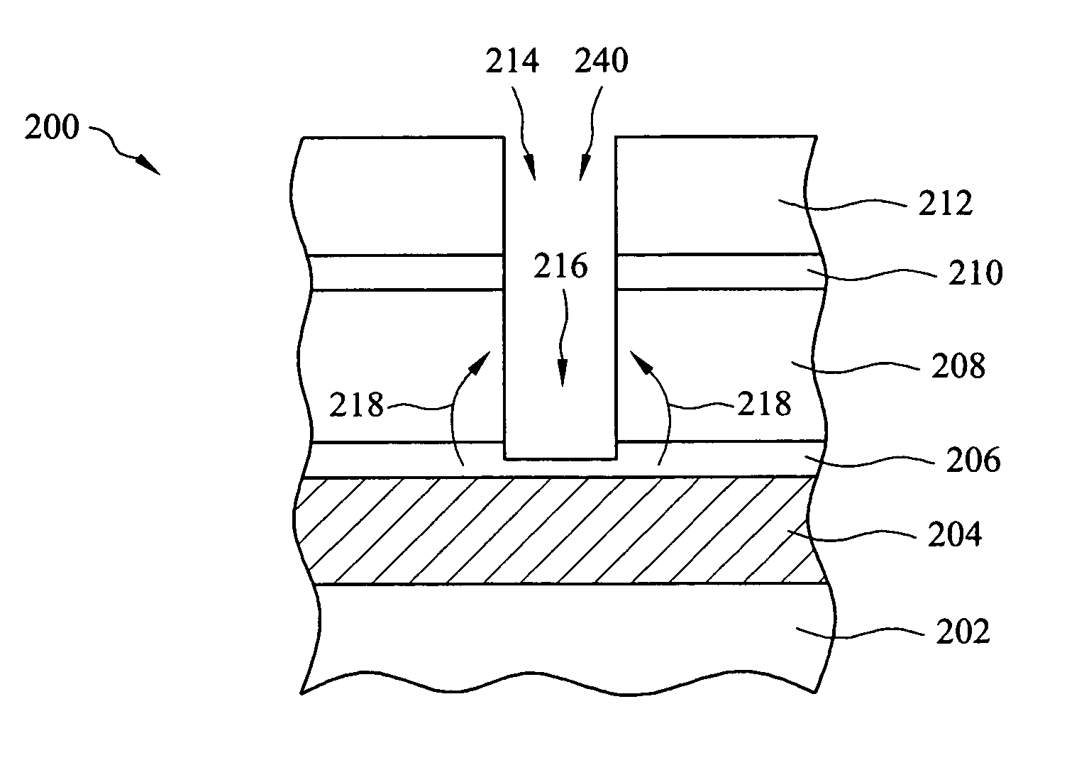
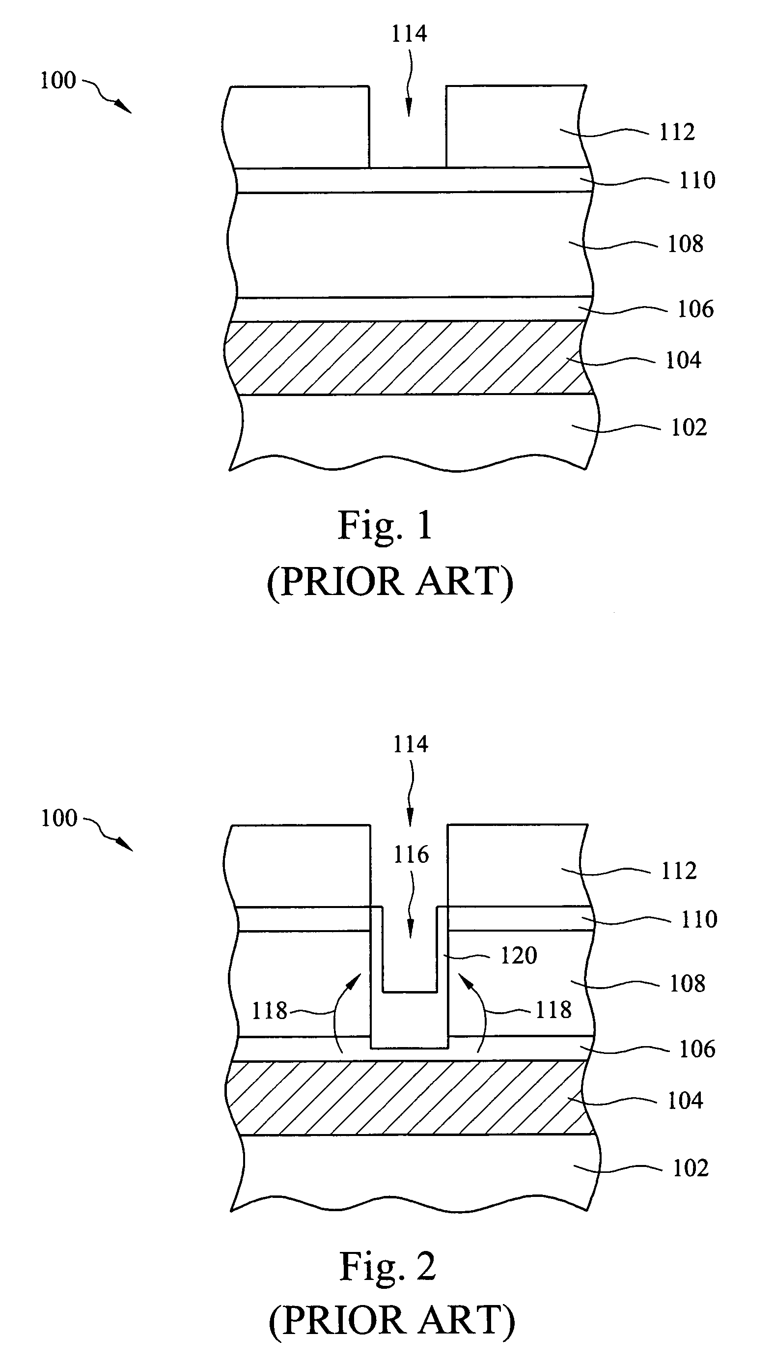
[0023]FIG. 1 shows a cross-sectional view of a prior art method of patterning a via trench or via pattern of a semiconductor device 100. A workpiece 102 is provided which may have circuit elements such as transistors and other devices formed thereon. A metallization layer may be formed over the workpiece 102 having conductive lines 104 formed therein. An etch stop layer 106 may be disposed over the metallization layer. An insulating layer 108 is formed over the workpiece 102, e.g., disposed over the etch stop layer 106, as shown. An anti-reflective coating (ARC) 110 may be disposed over the insulating layer 108.

[0024] To pattern the insulating layer 108 with via trenches, a layer of photoresist 112 is deposited over the insulating layer 108, e.g., over the anti-reflective coating 110, as shown. The layer of photoresist 112 is patterned with a desired pattern for one or more trenches, also shown.

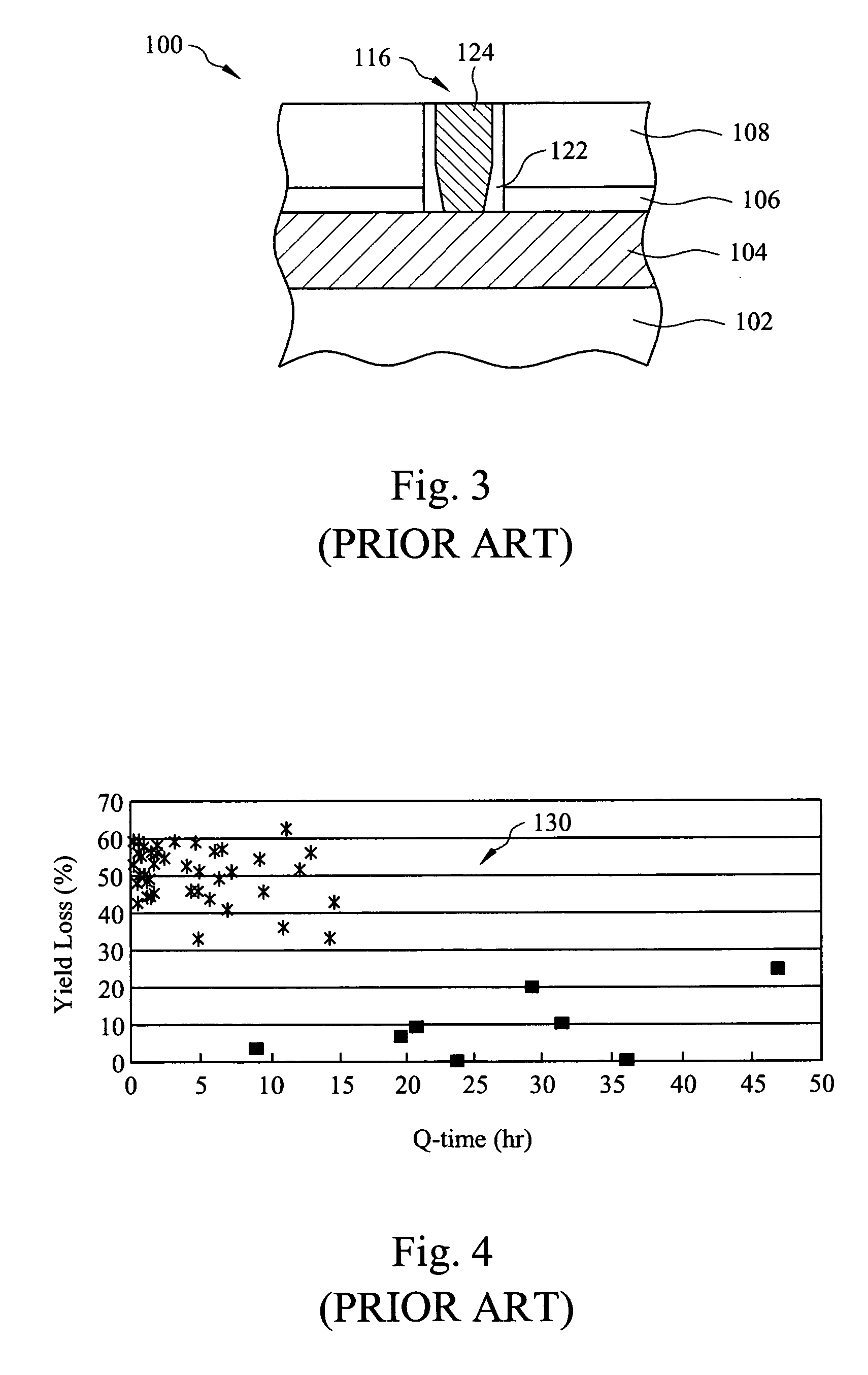
[0025] Referring next to FIG. 2, the layer of photoresist 112 is used as a mask while e...


PUM

PropertyMeasurementUnit
dielectric constantaaaaaaaaaa
timeaaaaaaaaaa
time periodaaaaaaaaaa

Abstract

Methods of preventing photoresist scum formation for etch processes for patterning material layers of semiconductor device material layers are disclosed. A treatment of N2 and O2 is used to prevent the formation of photoresist scum. The treatment may be performed in-situ, and may be performed during the etch process, after the etch process, or both. The treatment is particularly beneficial when implemented during the patterning of low dielectric constant material layers, and when used for the formation of isolated via patterns.

Description

TECHNICAL FIELD [0001] The present invention relates generally to the fabrication of semiconductor devices, and more particularly to methods of forming patterns in material layers using a layer of photoresist as a mask. BACKGROUND [0002] Semiconductor devices are used in a variety of electronic applications, such as personal computers, cell phones, digital cameras, and other electronic equipment, as examples. Semiconductor devices are typically fabricated by sequentially depositing insulating or dielectric layers, conductive layers, and semiconductive layers of material over a semiconductor substrate or workpiece, and patterning the various layers using lithography to form circuit components and elements thereon. [0003] One or more metallization layers are typically used to connect circuit components and elements together and to contact pads that may be used for external connection to the integrated circuit. If two or more metallization layers are used, vias are typically used to co...

Claims


Application Information

Patent Timeline
Patent Type & Authority Applications(United States)
IPC IPC(8): H01L21/4763
CPCH01L21/02063H01L21/31116H01L21/76834H01L21/76814H01L21/31138
Inventor CHU, YIN-SHENLEE, CHIA-PIAO
Owner TAIWAN SEMICON MFG CO LTD
Why Eureka
Eureka Blog
Learn More