Method for measuring diffraction patterns from a transmission electron microscopy to determine crystal structures and a device therefor

a transmission electron microscopy and crystal structure technology, applied in the direction of instruments, electrical appliances, material analysis, etc., can solve the problems of insufficient quantitative and precise structure analysis, poor crystallinity for precise x-ray structure determination, lack of dynamic range for recording intensity measurements of ed patterns, etc., to minimize the damage to radiation sensitive and non-radiation sensitive samples

Inactive Publication Date: 2007-02-01
SERGEEVICH AVILOV ANATOLY +1
View PDF7 Cites 26 Cited by
  • Summary
  • Abstract
  • Description
  • Claims
  • Application Information

AI Technical Summary

Benefits of technology

[0062] The present invention is a method and device that can interface to any TEM of the art or future TEM that enables said TEM to rapidly and precisely...

Problems solved by technology

Newly synthesised materials are often in powder form and often present poor crystallinity for precise X-Ray structure determination.
Such films are good for reproducing contrast detail in transmission electron microscope (TEM) imaging, for example, however, they suffer from lack of dynamic range for recording intensity measurements of ED patterns.
Therefore, they are not adequate for quantitative and precise structure analysis.
Despite the limitations, however, many different structures of organic and inorganic substances have been determined up to now using ED and photographic films, albeit with low resolution.
Another important issue when measuring ED data for resolving crystal structures is the speed at which intensities are measured.
Radiation damage to most samples usually occurs for exposures lasting longer than a minute.
Organic compounds are especially sensitive to radiation damage.
However, the scanning system has a lot of limitations.
Therefore, only very few beam resistant samples can be precisely me...

Method used


Image

  • Method for measuring diffraction patterns from a transmission electron microscopy to determine crystal structures and a device therefor
  • Method for measuring diffraction patterns from a transmission electron microscopy to determine crystal structures and a device therefor
  • Method for measuring diffraction patterns from a transmission electron microscopy to determine crystal structures and a device therefor

Examples


Embodiment Construction

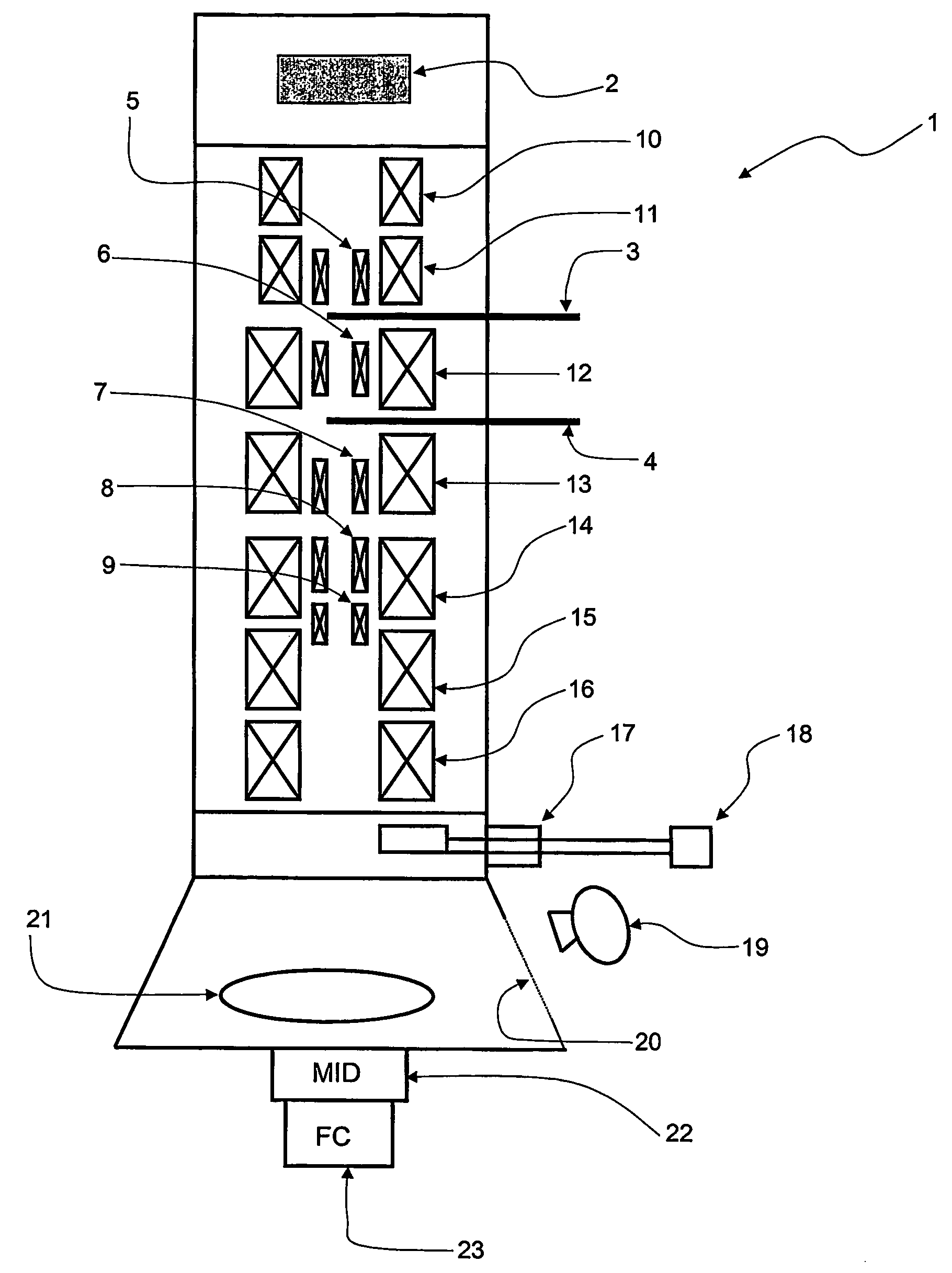
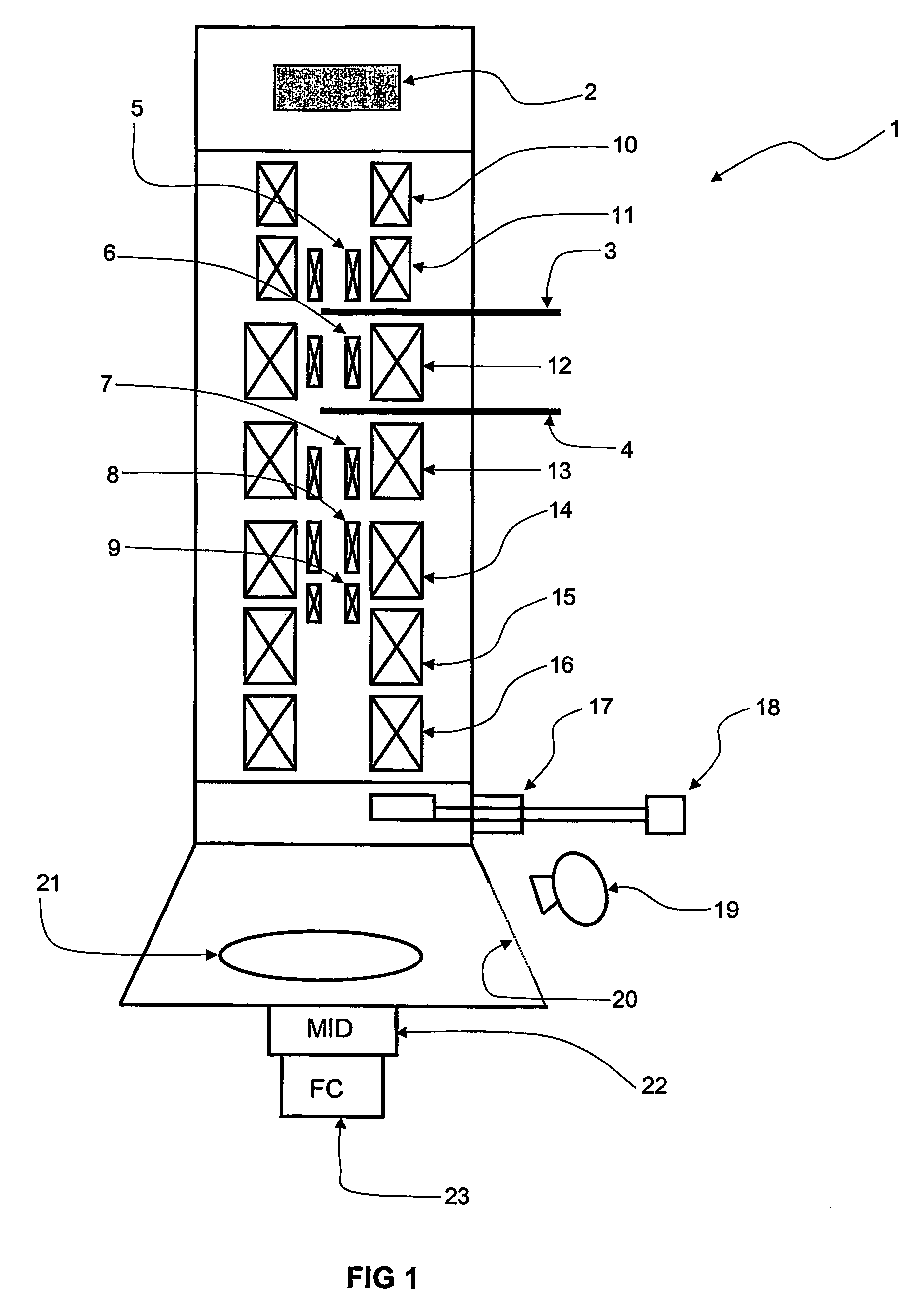
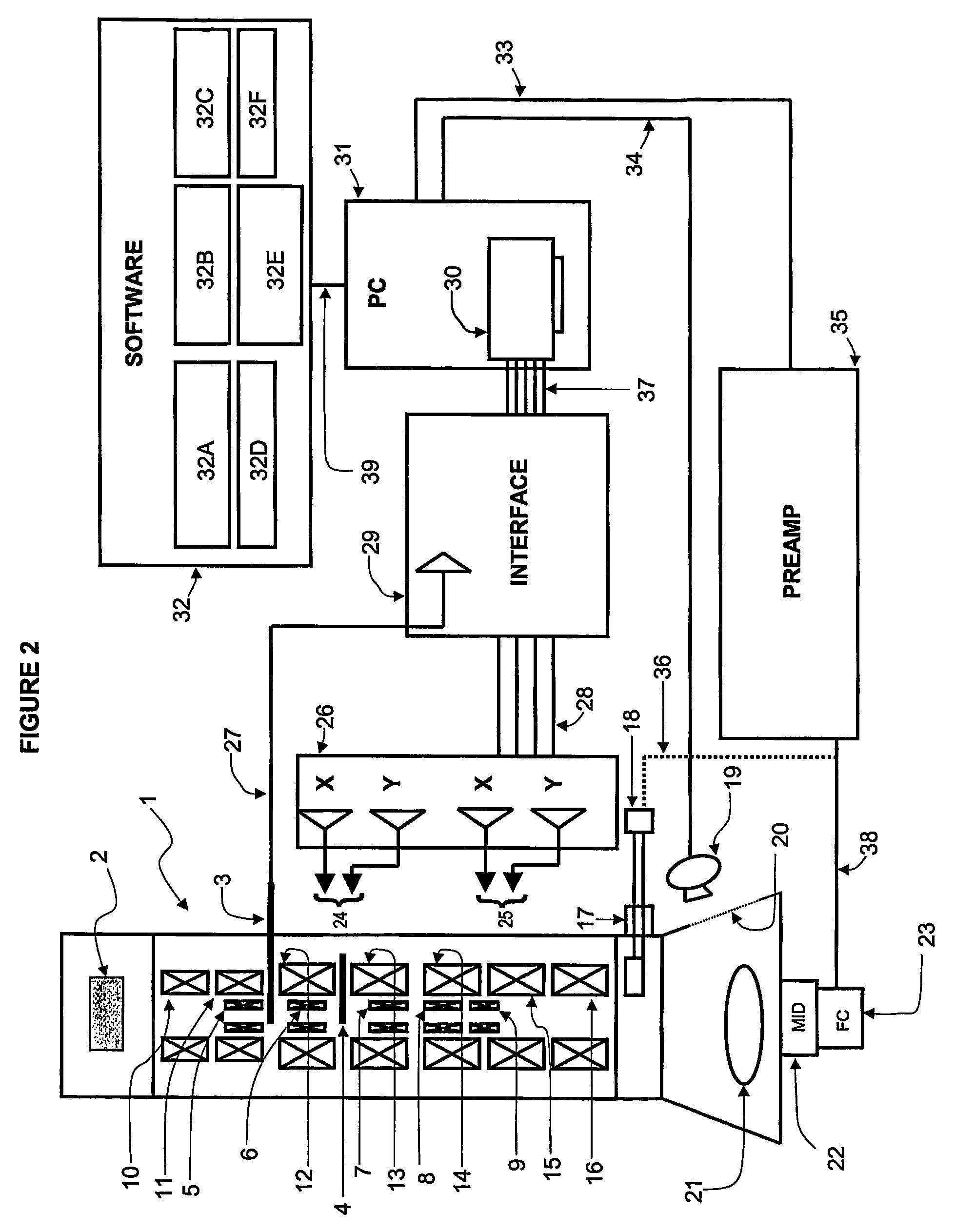
[0069] One embodiment of the present invention is a method for measuring electron diffraction (ED) patterns of a sample from a transmission electron microscope (TEM) wherein the ED pattern is scanned by means of deflector coils situated after the sample. The diffraction pattern is moved in a step-by-step scanning mode across a motionless (fixed) detector. The invention represents an improvement on the methods known in the art for scanning, such as, for example, that disclosed by Avilov et al, 1999 in relation to an EDC.

[0070] A sample according to the invention, is any substance susceptible to crystallographic study. Examples include nanocrystals, powders.

[0071] Another embodiment of the present invention is a method as disclosed herein wherein the electron beam is precessed by means of beam tilt coils in the TEM which are situated before the sample in combination with a similar precession of the ED pattern via deflection coil below the sample (Vincent and Midgley 1998). The measu...


PUM


Abstract

A device and method which enable a transmission electron microscope to measure electron diffraction patterns of a sample very precisely are disclosed. The patterns are suitable for structure determination. The electron beam is precessed by means of deflector coils (6) in the transmission electron microscope before the sample (4), in combination with a similar precession of the electron diffraction pattern by means of deflector coils (9) situated after the sample. The electron diffraction pattern is scanned by means of deflector coils (9) situated after the sample.

Description

BACKGROUND OF THE INVENTION [0001] The macroscopic material world is formed by millions of crystals; every crystal at a microscopic level is formed by a cell having some symmetry for example hexagonal, trigonal, cubic etc, and having a specified quantity of atoms therein whose positions are defined. In order to understand the properties of matter is essential to know the crystal structure at atomic level; this requires atomic resolution structural studies by means of X-Rays, neutron or electron diffraction. [0002] X-Ray diffraction is a technique which provides an average structure, usually of tens of thousands of particles. Newly synthesised materials are often in powder form and often present poor crystallinity for precise X-Ray structure determination. [0003] Electron diffraction (ED) is much more sensitive than X-Ray diffraction, providing about a ten thousand fold enhancement in signal. Electron diffraction structure analysis of materials originally developed in the early 50's ...

Claims


Application Information

Patent Timeline
IPC IPC(8): G21K7/00G01N23/20H01J37/295
CPCH01J37/295G01N23/20058
Inventor SERGEEVICH, AVILOV ANATOLYVLADIMIROVICH, KULIGIN KIRILL
Owner SERGEEVICH AVILOV ANATOLY
Why Eureka
Try Eureka