Nonvolatile memory semiconductor device and method for manufacturing same

Active Publication Date: 2007-02-01
RENESAS ELECTRONICS CORP
View PDF6 Cites 9 Cited by
  • Summary
  • Abstract
  • Description
  • Claims
  • Application Information

AI Technical Summary

Benefits of technology

[0010] According to the present invention, a nonvolatile memory semiconductor device and a method for manufacturing thereof are provided to avoid d

Problems solved by technology

In addition to above, when concentration of atomic nitrogen in the tunnel insulating film is lower than 0.1 atomic

Method used


Image

  • Nonvolatile memory semiconductor device and method for manufacturing same
  • Nonvolatile memory semiconductor device and method for manufacturing same
  • Nonvolatile memory semiconductor device and method for manufacturing same

Examples


Example

FIRST EMBODIMENT

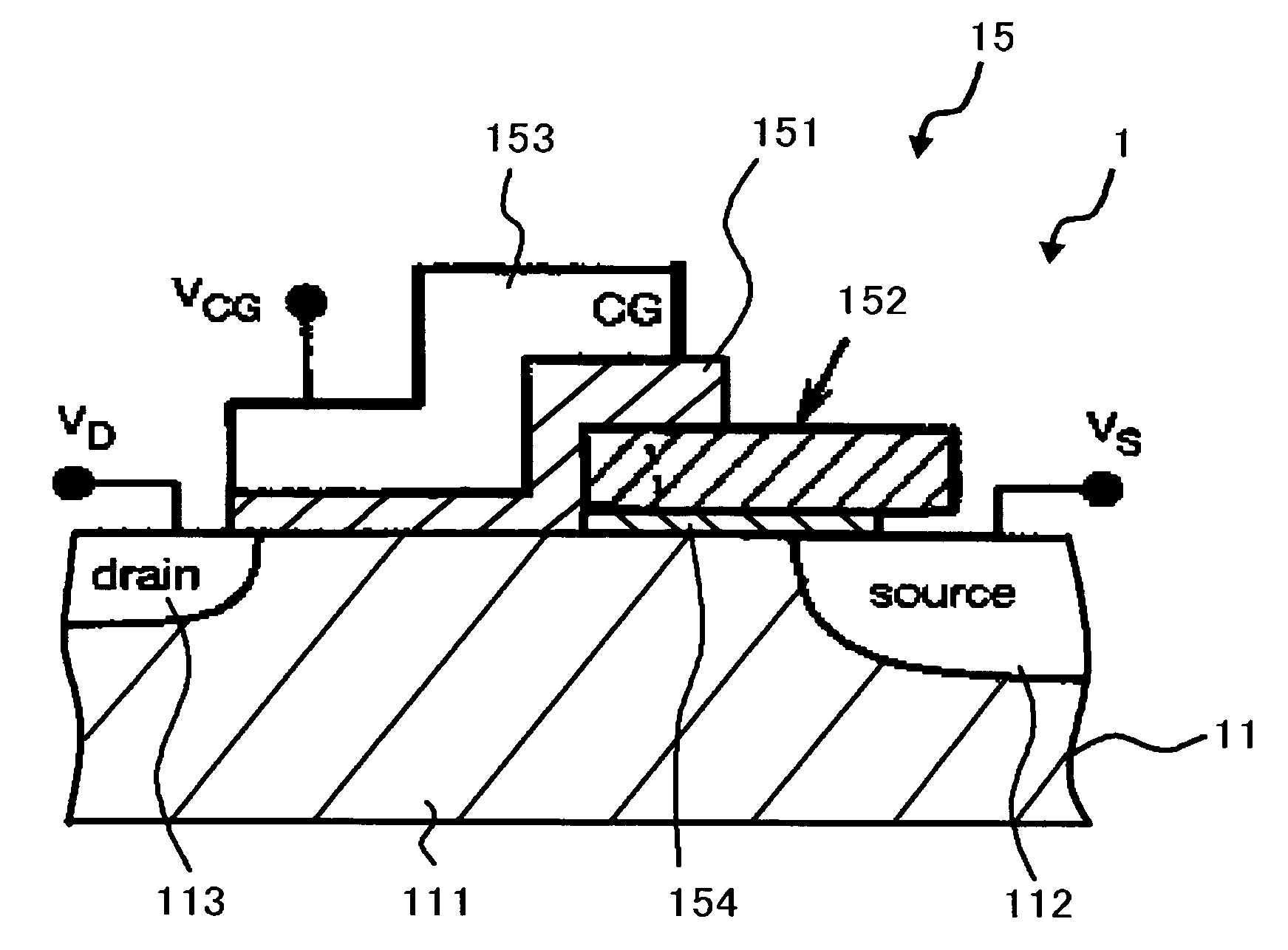
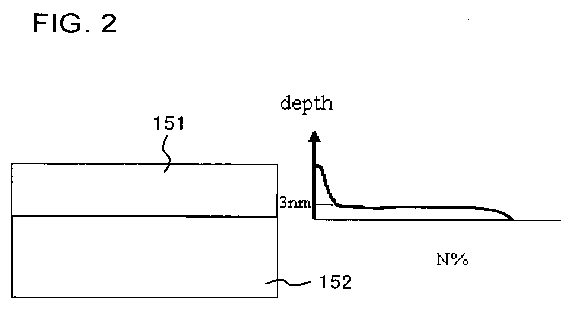
[0027] A nonvolatile memory semiconductor device 1 of the present embodiment is shown in FIG. 1. The nonvolatile memory semiconductor device 1 includes a silicon substrate 11 composed of a semiconductor substrate and a memory cell 15 disposed on the silicon substrate 11. The memory cell 15 includes a floating gate 152 formed on the silicon substrate 11 through an insulating film 154 therebetween, a tunnel insulating film 151 provided on this floating gate 152 and disposed adjacent to the floating gate 152, and a control gate 153 provided on the tunnel insulating film 151.

[0028] A p-type well 111 is formed in the silicon substrate 11 by ion implanting a p-type impurity. In addition, an n-type source region 112 and an n-type drain region 113 are formed a region in the p-type well 111 located in the side of the tunnel insulating film 151.

[0029] The tunnel insulating film 151 is disposed between the floating gate 152 and the control gate 153, and provided to contact w...

Example

SECOND EMBODIMENT

[0070] A nonvolatile memory semiconductor device 2 of the present embodiment is shown in FIG. 12. The nonvolatile memory semiconductor device 2 includes a silicon substrate 21 composed of a semiconductor substrate and a memory cell 25 disposed on the silicon substrate 21. The memory cell 25 includes a tunnel insulating film 251 composed of a silicon oxide film containing nitrogen provided on the silicon substrate 21, a floating gate 252 disposed on such tunnel insulating film 251 and adjacent to the tunnel insulating film 251, and the control gate 253 provided to be capacitively coupled to the aforementioned floating gate 252 through an insulating film 254. A p-type well 211 is formed in the silicon substrate 21 by ion implanting a p-type impurity. In addition, an n-type source region 212 and an n-type drain region 213 are formed a region in the p-type well 211 located in the side of the tunnel insulating film 251. Concentration of atomic nitrogen in the tunnel ins...


PUM


Abstract

A nonvolatile memory semiconductor device and a method for manufacturing thereof are provided to avoid deterioration of the tunnel insulating film to increase frequency of writing data on the nonvolatile memory semiconductor device and erasing thereof. Concentration of atomic nitrogen in a tunnel insulating film 151 of a nonvolatile memory semiconductor device 1 is 0.1 to 5 atomic %. In addition, larger amount of atomic nitrogen in the tunnel insulating film 151 is distributed primarily in the interface layer of the tunnel insulating film 151, and concentration of atomic nitrogen in the interface layer is 10 times or more higher than concentration of atomic nitrogen in other portion of the tunnel insulating film 151. Further, density per unit area of atomic nitrogen in the surface of the tunnel insulating film 151 contacting with the floating gate is equal to or lower than 4×10¹⁴ atoms/cm2.

Description

[0001] This application is based on Japanese patent application No. 2005-218,970, the content of which is incorporated hereinto by reference. BACKGROUND [0002] 1. Field of The Invention [0003] The present invention relates to a nonvolatile memory semiconductor device and a method for manufacturing thereof. [0004] 2. Related Art [0005] In the conventional technologies, a method for preventing deterioration of a gate insulating film or a tunnel insulating film by doping nitrogen to a gate insulating film of a metal oxide semiconductor (MOS) transistor or a tunnel insulating film of a nonvolatile memory semiconductor device to prevent from an electron trap is proposed (see, for example, Japanese Patent No. 3,264,265). The tunnel insulating film of the nonvolatile memory semiconductor device maintains electron in a floating gate. On the contrary, a tunneling current flows through the aforementioned tunnel insulating film in each time a writing or an erasing data is conducted. Therefore,...

Claims


Application Information

Patent Timeline
IPC IPC(8): H01L29/76
CPCH01L29/42324H01L29/7885H01L29/51
Inventor CHO, SHIEN
Owner RENESAS ELECTRONICS CORP
Why Eureka
Try Eureka