Organic thin film transistor display panel

a technology of organic thin film transistors and array panels, which is applied in the field of organic thin film transistor array panels, can solve the problems of complex layered structure of conventional otft array panels, and the inability to meet the requirements of organic semiconductor manufacturing

Inactive Publication Date: 2007-02-01
SAMSUNG ELECTRONICS CO LTD
View PDF11 Cites 20 Cited by
  • Summary
  • Abstract
  • Description
  • Claims
  • Application Information

AI Technical Summary

Problems solved by technology

However, the manufacturing process for an organic semiconductor is more sensitive to process conditions than for inorganic semiconductors.
Accordingly, conventional OTFT array panels may have complicated layered structures and need additional process steps for reducing the degradation of OTFTs.

Method used


Image

  • Organic thin film transistor display panel
  • Organic thin film transistor display panel
  • Organic thin film transistor display panel

Examples


Embodiment Construction

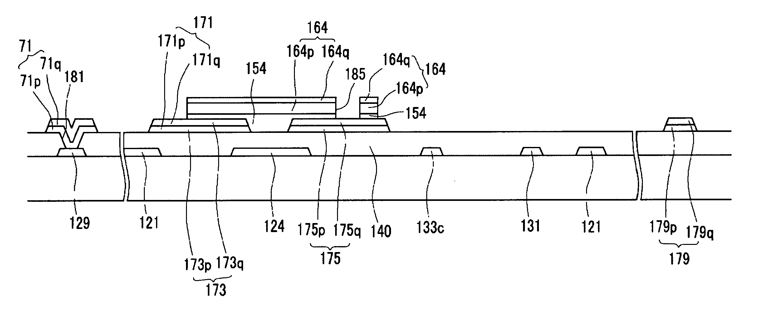
[0016] In the drawings, the thickness of layers and regions are exaggerated for clarity. Like numerals refer to like elements throughout. It will be understood that when an element such as a layer, region or substrate is referred to as being “on” another element, it can be directly on the other element or intervening elements may also be present. In contrast, when an element is referred to as being “directly on” another element, there are no intervening elements present.

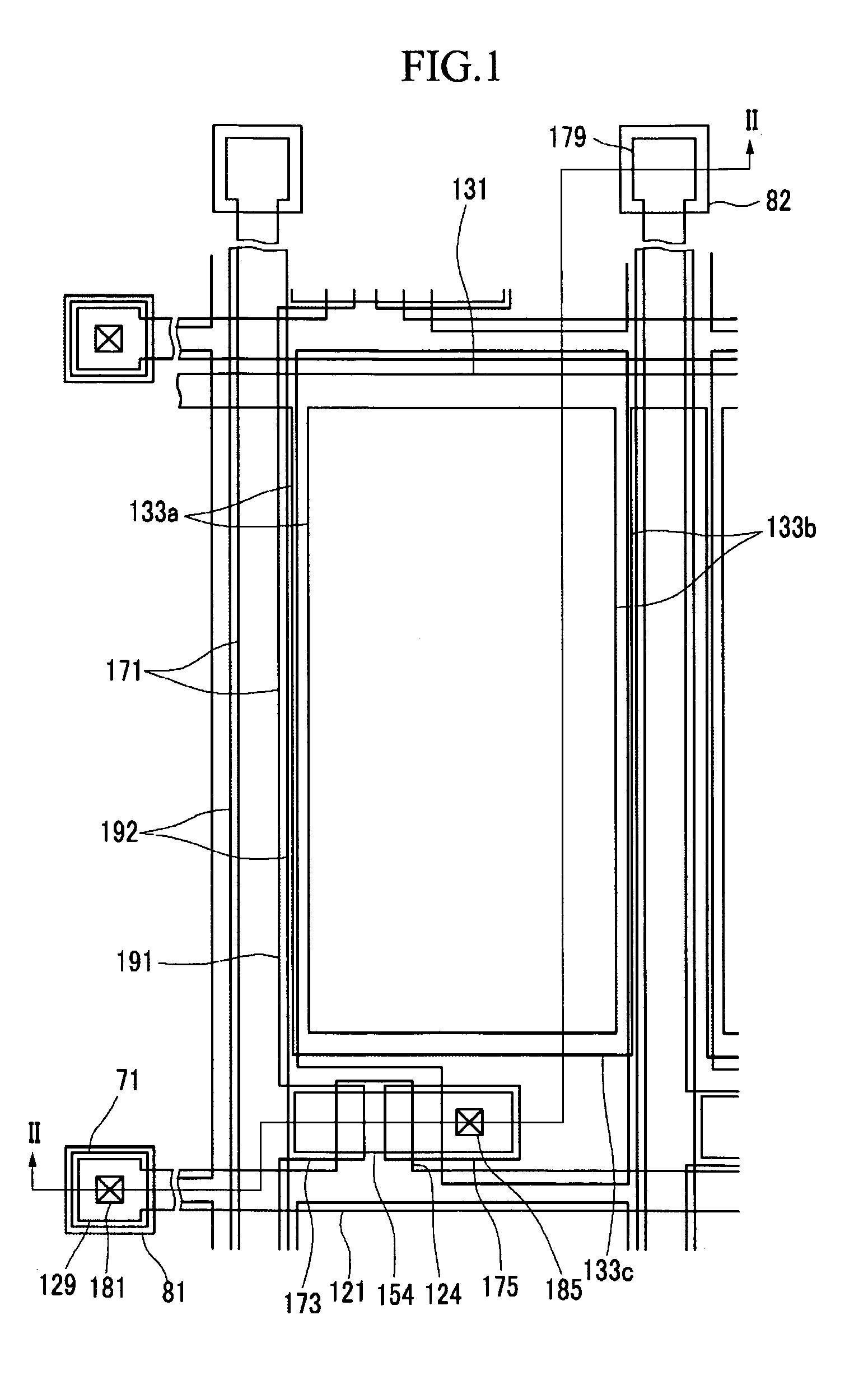
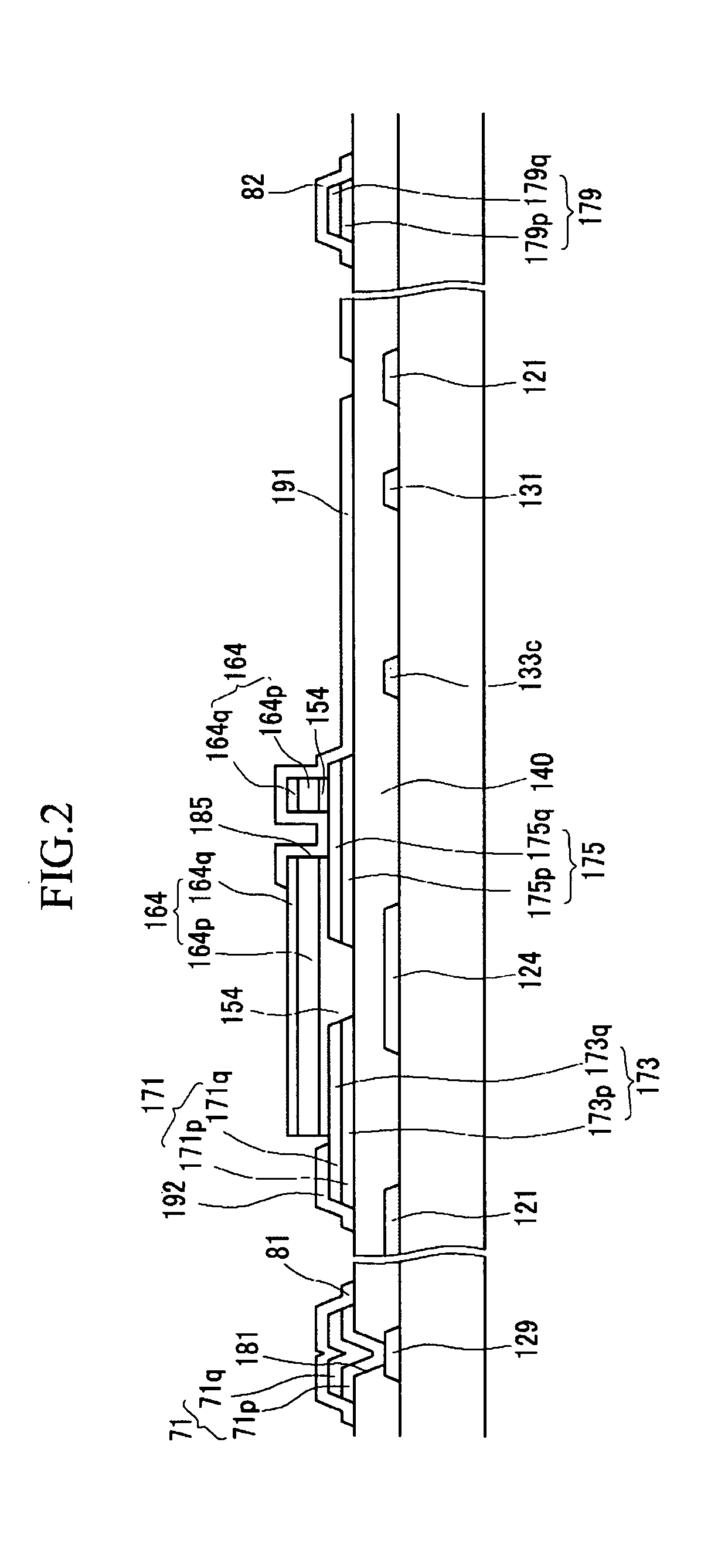
[0017]FIG. 1 is a layout view of a TFT array panel for a liquid crystal display according to an embodiment of the present invention, and FIG. 2 is a sectional view of the TFT array panel shown in FIG. 1 taken along the line II-II. A plurality of gate lines 121 and a plurality of storage electrode lines 131 are formed on an insulating substrate 110 such as transparent glass or plastic.

[0018] Gate lines 121 transmit gate signals and extend substantially in a transverse direction. Each of gate lines 121 includes a plu...


PUM

PropertyMeasurementUnit
temperatureaaaaaaaaaa
inclination angleaaaaaaaaaa
temperatureaaaaaaaaaa

Abstract

An organic thin film transistor array panel according to an embodiment of the present invention includes forming a gate line on an insulating plastic or glass substrate; forming a gate insulating layer on the gate line; forming a data line and a drain electrode on the gate insulating layer, the data line and the drain electrode comprising a first conductive film and a second conductive film of indium tin oxide (ITO) or indium zinc oxide (IZO) that has a work function similar to that of the organic semiconductor that is deposited overlapping the data line and the drain electrode; forming a passivation layer on the organic semiconductor; and forming a pixel electrode connected to the drain electrode on the passivation and the gate insulating layer.

Description

CROSS-REFERENCE TO RELATED APPLICATION [0001] This Application claims priority from Korean patent application number 10-2005-0069351 filed on Jul. 29, 2005, and all the benefits accruing therefrom under 35 U.S.C. §119, the contents of which are incorporated by reference herein. FIELD OF THE INVENTION [0002] The present invention relates to an organic thin film transistor array panel and a manufacturing method thereof. DESCRIPTION OF RELATED ART [0003] Organic thin film transistors (OTFT) employ an organic active layer instead of inorganic semiconductor such as silicon. Since an organic semiconductor can be easily deposited at a low temperature by a solution process, etc., it is more suitable for large flat panel displays than inorganic semiconductor that use chemical vapor deposition. In addition, since organic material can be easily formed of fiber or film, OTFTs can be used with flexible display devices. [0004] However, the manufacturing process for an organic semiconductor is mor...

Claims


Application Information

Patent Timeline
Patent Type & Authority Applications(United States)
IPC IPC(8): G02F1/136
CPCH01L27/283H01L51/102H01L51/0545H10K19/10H10K10/82H10K10/466H05B33/26H05B33/10
Inventor SONG, KEUN-KYULEE, YONG-UK
Owner SAMSUNG ELECTRONICS CO LTD
Why Eureka
Try Eureka