Memory device and method having separate write data and read data buses

a memory device and data bus technology, applied in the field of memory devices, can solve the problems of increasing the memory devices have not been able to keep up with the increase in data bandwidth of memory controllers and memory data buses, and reducing hardware limitations adds cost, power, and/or size to the memory

Inactive Publication Date: 2007-02-01
MICRON TECH INC
View PDF57 Cites 63 Cited by
  • Summary
  • Abstract
  • Description
  • Claims
  • Application Information

AI Technical Summary

Problems solved by technology

Generally, bandwidth limitations are not related by memory controllers typically coupled to memory devices since the memory controllers sequence data to and from the memory devices as fast as the memory devices allow.
However, memory devices have not been able to keep up with increases in the data bandwidth of memory controllers and memory data buses.
Although these hardware limitations can be reduced to some degree through the design of the memory device, a compromise must be made because reducing the hardware limitations typically adds cost, power, and/or size to the memory devices, all of which are undesirable alternatives.
While memory devices can rapidly handle “well-behaved” accesses at ever increasing rates, for example, sequel traffic to the same page of a memory device, it is much more difficult for the memory devices to resolve “badly-behaved traffic,” such as accesses to different pages or banks of the memory device.
In addition to the limited bandwidth of memory devices, the performance of computer systems is also limited by laten

Method used


Image

  • Memory device and method having separate write data and read data buses
  • Memory device and method having separate write data and read data buses
  • Memory device and method having separate write data and read data buses

Examples


Embodiment Construction

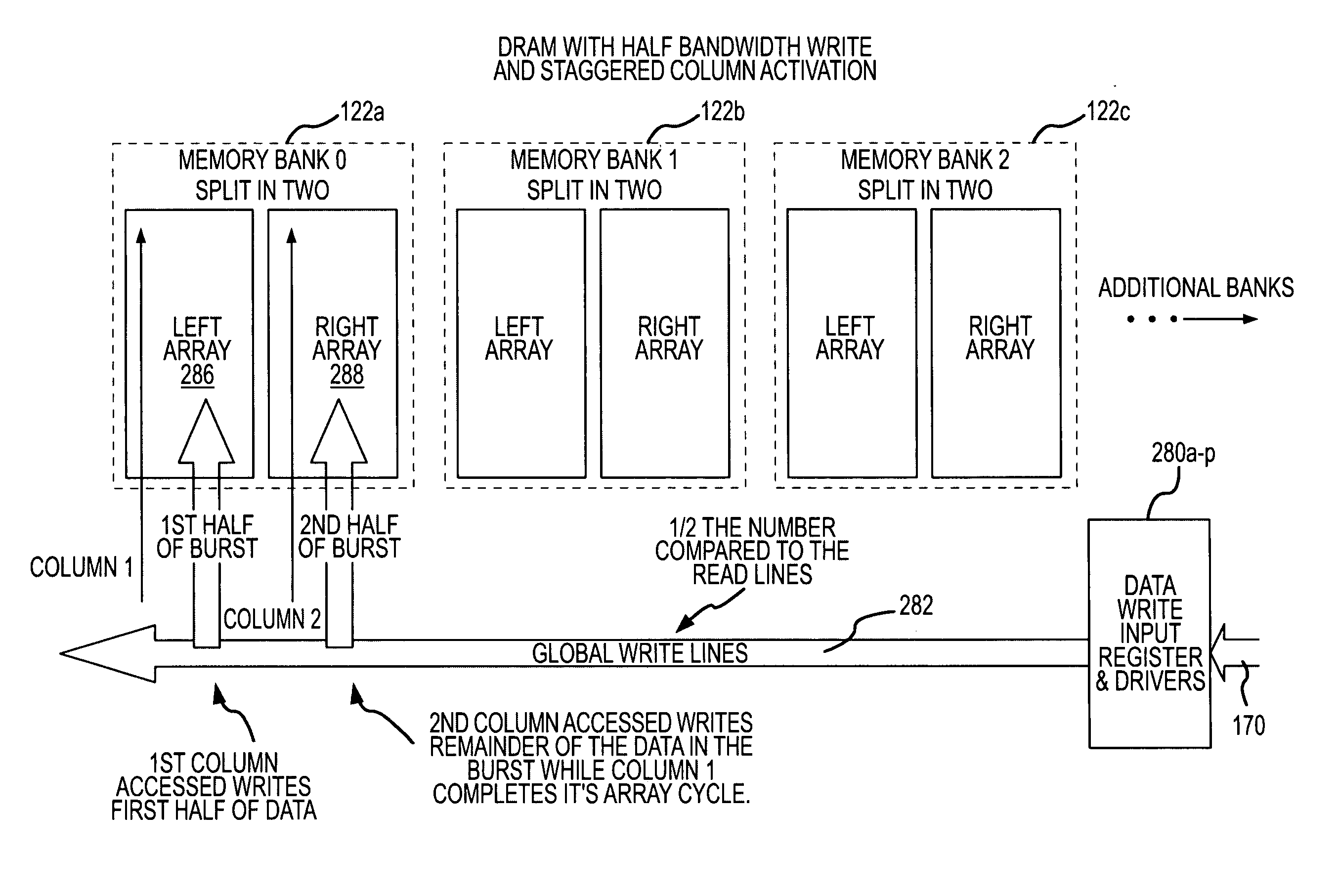
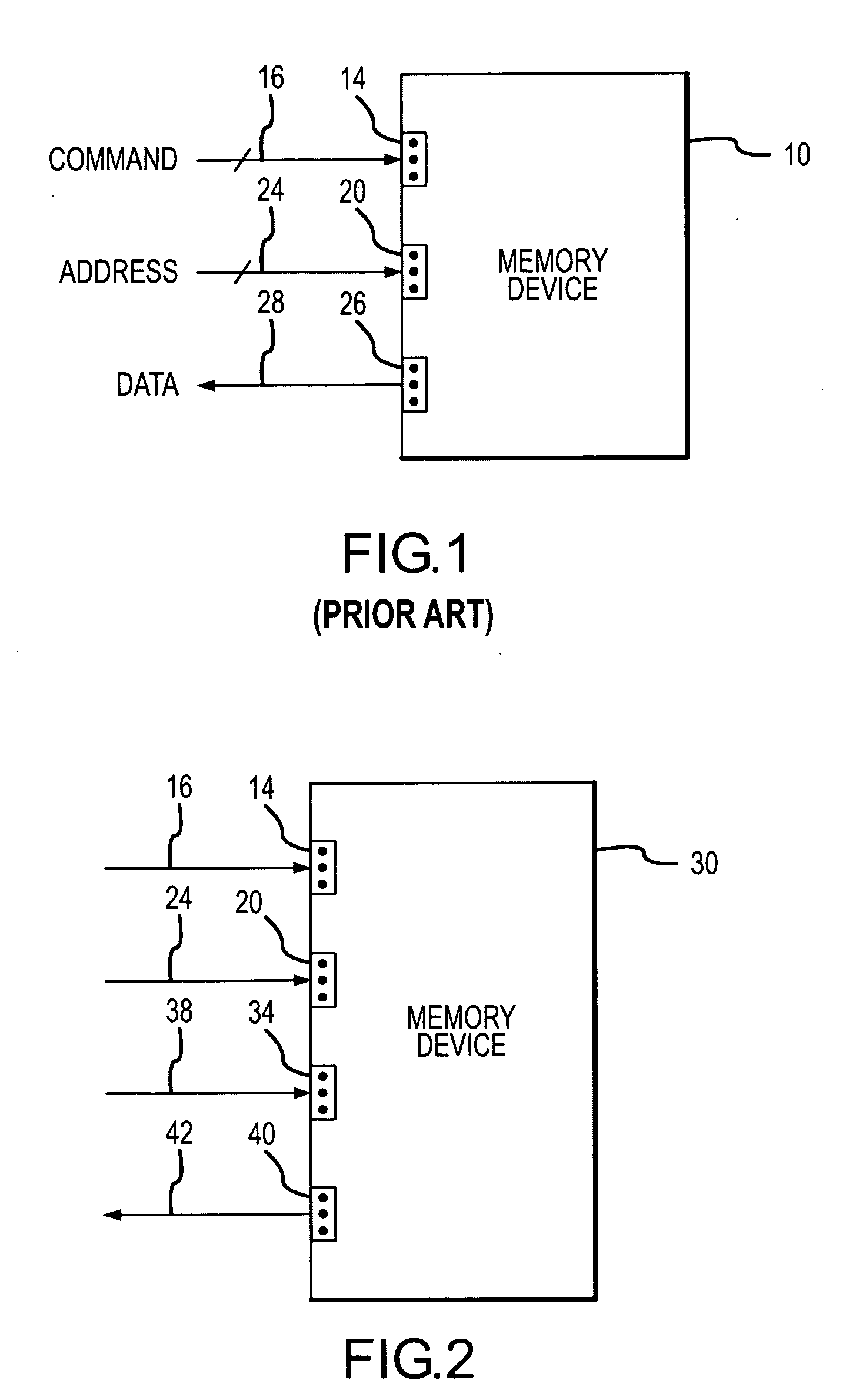
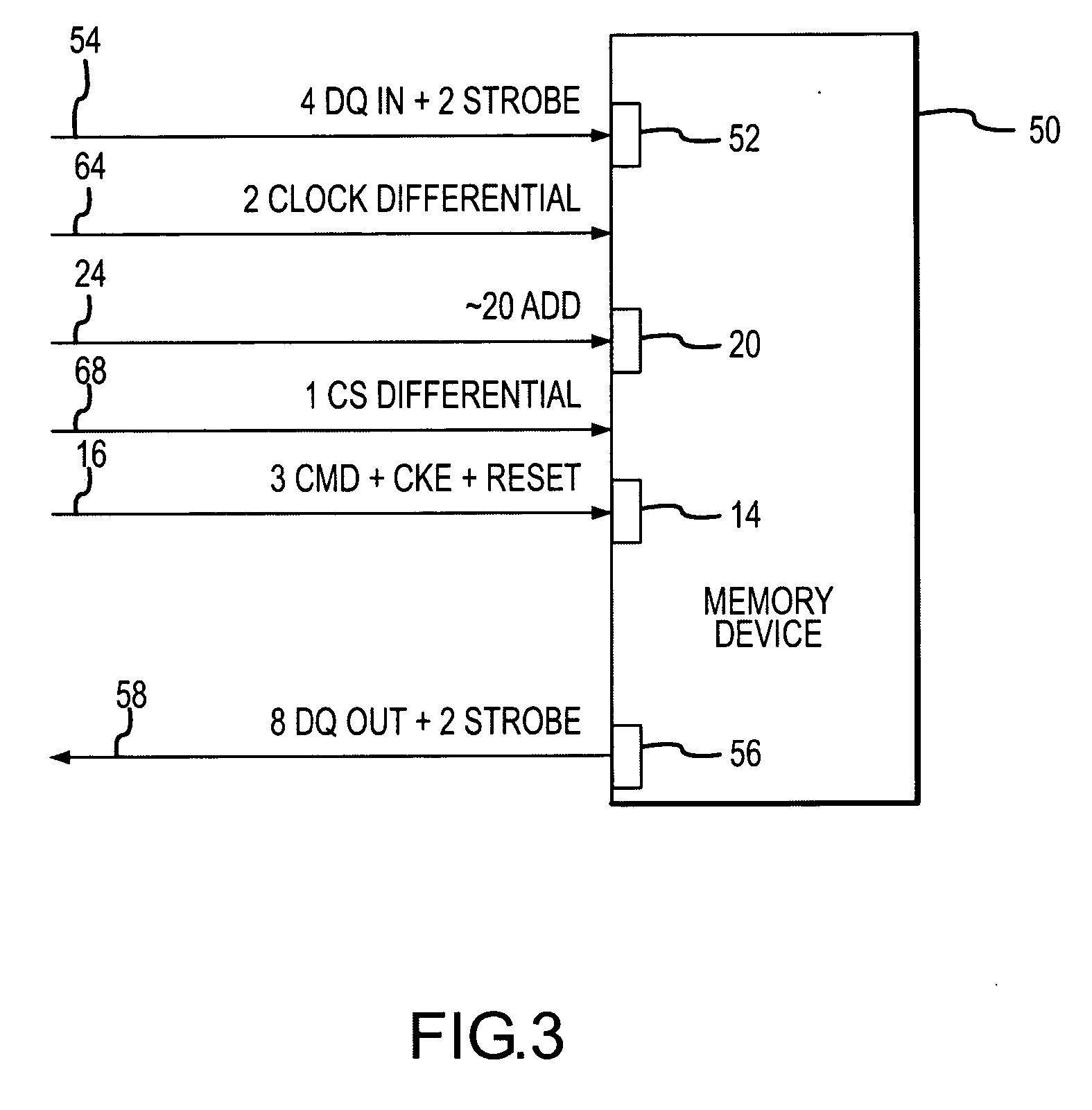
[0025] A memory device 50 according to one embodiment of the invention is shown in FIG. 3. The memory device 50 may be a DRAM device, and SRAM device, a ROM device, a flash memory device, or some other type of memory device. The memory device 50, like the memory devices 10, 30, includes a set of command terminals 14 coupled to a command bus 16, In the example shown in FIG. 3, the command bus 16 has a width of five bits for coupling 3 command bits, a clock enable (“CKE”) signal, and a reset signal to the memory device 50. The memory device 50 also includes a set of address terminals 20 coupled to an address bus 24. The memory device 50, like the memory device 30, includes a set of write data terminals 52 coupled to a write data bus 54 and a set of read data terminals 56 coupled to a read data bus 58. However, unlike the write data bus 38 and read data bus 42 coupled to the memory device 30 as shown in FIG. 2, the width of the write data bus 54 is not the same as the width of the read...


PUM


Abstract

A synchronous dynamic random access memory (“SDRAM”) device includes several banks of memory cell coupled to a read data path and a write data path. The read data path includes a read latch that stores a relatively large number of read data bits received in parallel from a bank of memory cells. Groups of the stored read data bits are sequentially selected by a multiplexer and applied to a read data bus. Groups of write data bits are sequentially coupled to the SDRAM device through a write data bus that is separate from the read data bus, and they are sequentially stored in input registers. When the input registers are full, the write data bits are coupled in parallel to a bank of memory cells. The number of bits in the write data bus is preferably a submultiple of the number of bits in the read data bus.

Description

TECHNICAL FIELD [0001] This invention relates to memory devices, and, more particularly, to a memory device having separate unidirectional write and read data buses. BACKGROUND OF THE INVENTION [0002] Memory devices are commonly used in a wide variety of electronic devices, such as personal computers. A memory device 10, such as a dynamic random access memory (“DRAM”) device, a static random access memory (“SRAM”) device, a flash memory device, or another type of memory device, is shown in FIG. 1. The memory device 10 includes a set of command terminals 14, which is typically connected to a command bus 16, a set of address terminals 20, which is typically connected to an address bus 24, and a set of data terminals 26, and which is typically the connected to a data bus 28. The command bus 16 and the address bus 24 are unidirectional buses while the data buses 28 is a bidirectional bus. [0003] In operation, command signals corresponding to a memory command, such as a read or a write c...

Claims


Application Information

Patent Timeline
IPC IPC(8): G06F12/06G06F12/00
CPCG06F13/1684G11C7/1018G11C7/1051G11C7/106G11C7/1072G11C2207/107G11C7/1087G11C8/12G11C8/18G11C11/4093G11C7/1078
Inventor JANZEN, JEFFWRIGHT, JEFFREYCULLUM, JAMES
Owner MICRON TECH INC
Why Eureka
Try Eureka